Stacked chip and test method of stacked chip

A test method and chip technology, which can be used in electronic circuit testing, measuring device casings, etc., can solve problems such as large resource consumption

Pending Publication Date: 2022-04-08
XI AN UNIIC SEMICON CO LTD
View PDF0 Cites 0 Cited by
  • Summary
  • Abstract
  • Description
  • Claims
  • Application Information

AI Technical Summary

Problems solved by technology

[0008] The main purpose of this application is to provide a stacked chip and a stacked chip testing method to solve the problem in the prior art that multiple chips in a stacked chip require multiple test machines, resulting in large resource consumption

Method used


Image

  • Stacked chip and test method of stacked chip
  • Stacked chip and test method of stacked chip
  • Stacked chip and test method of stacked chip

Examples


Embodiment 1

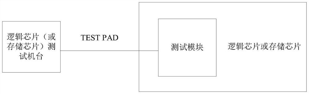
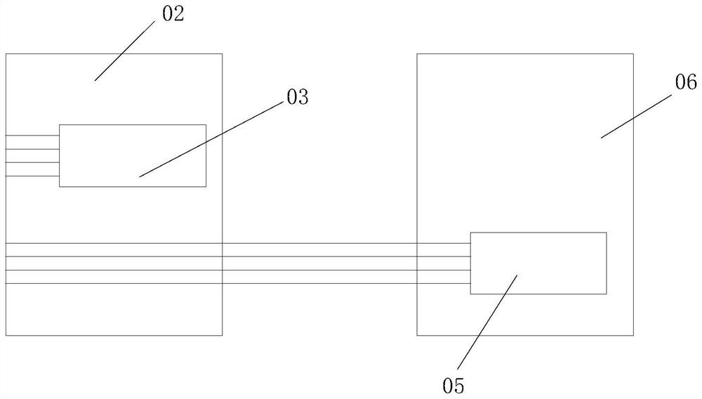
[0074] In a specific embodiment of the present application, such as Figure 4 As shown, the stacked chip system includes: a testing machine 01, a first chip 02, and a second chip 06, wherein the first chip 02 is a logic chip, the second chip 06 is a memory chip, and the logic chip includes two test modules, namely the first test module 03 and the second test module 05, namely the BIST test module and the DFT test module, and a first multiplexer 07, namely the MUX module, the DFT test module in the logic chip and the storage The chips are electrically connected, and the test machine 01 can test the memory chip through the external interface of the DFT test module. The specific test process is as follows: the test machine 01 sends out two sets of test signals, and the MUX module judges according to the received test signals. The test module corresponding to the test signal is obtained, and one group of test signals is input to the BIST test module (ie the first test module 03) i...

Embodiment 2

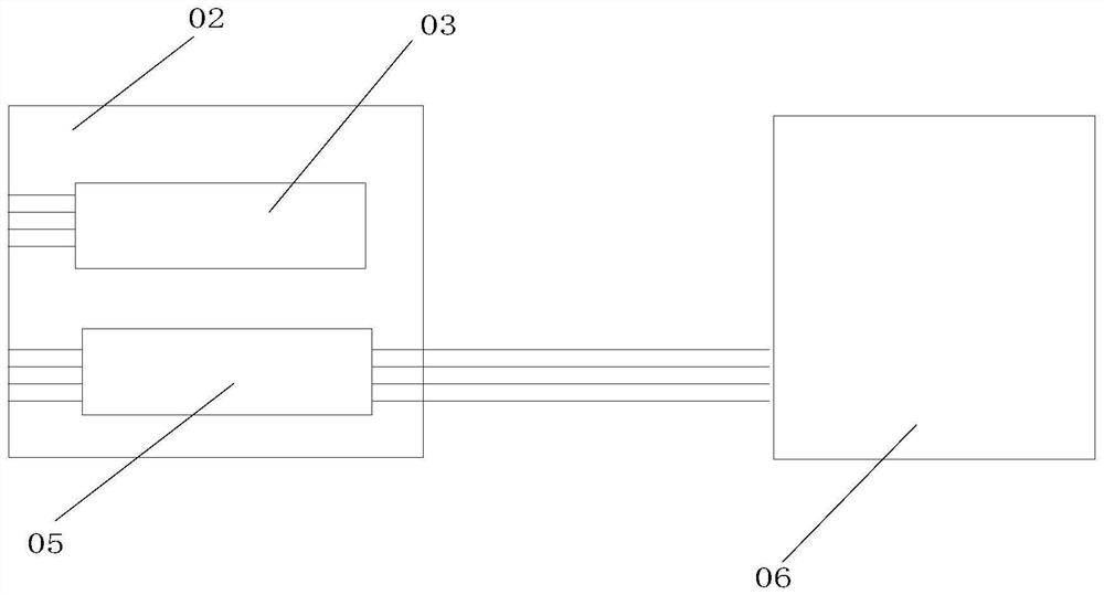
[0076] In another specific embodiment of the present application, such as Figure 5 As shown, the stacked chip system includes: a test station 01 , a first chip 02 , a second chip 06 , a third chip 09 , a first multiplexer 07 and a second multiplexer 08 , wherein, the first chip 02 integrates three test modules, namely the first test module 03 , the second test module 05 and the third test module 10 , that is, the first test module 03 is used to test the first chip 02 , the second test module 05 is used to test the second chip 06, the third test module 10 is used to test the third chip 09, the second multiplexer 08 is located in the first chip 02, the second multiplexer One end of the device 08 is electrically connected to the second test module 05 and the third test module 10 respectively, and the other end of the second multiplexer 08 is electrically connected to the second chip 06 and the third chip 09 respectively. The specific test process is as follows: For the test The...


PUM


Abstract

The invention provides a stacked chip and a test method of the stacked chip, the stacked chip comprises a plurality of chips, the plurality of chips at least comprise a first chip, the first chip comprises at least one input / output interface, one end of the input / output interface is used for receiving at least one group of test signals sent by a test machine, and the other end of the input / output interface is used for receiving at least one group of test signals sent by the test machine. The other ends of the input and output interfaces are electrically connected with test modules of a plurality of chips respectively, a group of test signals output by the input and output interfaces are input to the corresponding test modules, and each test module is connected with at least one input and output interface; therefore, a plurality of chips can be tested at the same time only by inputting a plurality of groups of test signals to the input / output interface of the first chip through one test machine. According to the scheme, the test cost can be reduced, high test efficiency is guaranteed, and therefore the problem that in the prior art, multiple chips in stacked chips need multiple test machines, and consequently resource consumption is large is solved.

Description

technical field [0001] The present application relates to the field of stacked chip testing, and in particular, to a stacked chip and a method for testing stacked chips. Background technique [0002] The chip testing process is a key area of ​​the semiconductor industry. Chip testing includes wafer testing, and the main purpose is to pick out defective chips in the wafer. During the wafer testing process, the chips need to be tested for electrical performance to ensure that the chips on the wafer are qualified products before packaging. [0003] The three-dimensional stacking platform is a technology that connects logic chips and memory chips through hybrid bonding technology to realize near-memory computing. The platform is mainly composed of three parts: logic chip, memory chip and connection layer. Compared with a single logic (or memory) chip, the three-dimensional stacked platform contains both logic chips and memory chips. Therefore, when conducting electrical perfor...

Claims


Application Information

Patent Timeline
IPC IPC(8): G01R1/04G01R31/28
Inventor 左丰国王玉冰李岩刘琦韩洋邱锋波
Owner XI AN UNIIC SEMICON CO LTD
Why Eureka
Try Eureka