Semiconductor device electrode manufacturing method and semiconductor device
A manufacturing method and semiconductor technology, applied in the direction of semiconductor devices, circuits, electrical components, etc., can solve the problems affecting the performance of semiconductor chips, electrode oxidation and corrosion, and inability to protect the metal electrode layer well, so as to prevent corrosion and save energy. Cost and effect of reducing the forming process
- Summary
- Abstract
- Description
- Claims
- Application Information
AI Technical Summary
Problems solved by technology
Method used
Image

Examples
Embodiment 1
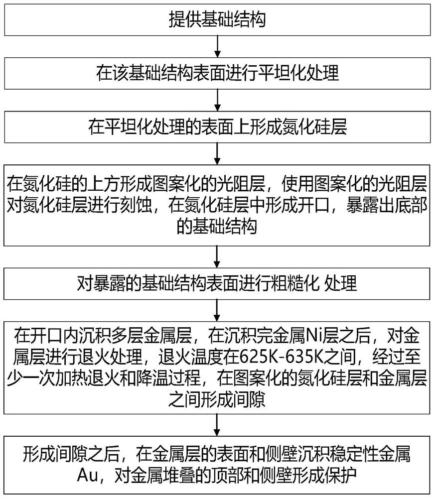
[0065] A method for manufacturing a metal electrode of an LED device, comprising the steps of:
[0066] 1) Provide traditional outdoor LCD display LED chips as the basic structure 1;
[0067] 2) Grinding the upper surface of the LED chip to a roughness of 0.5 nm by chemical mechanical polishing;
[0068] 3) Using CVD to grow 5000 Å on the upper surface of the above-mentioned LED chip thick hard compound layer 2;
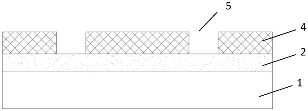
[0069] 4) Coating photoresist on the surface of the hard compound layer 2, and baking at 95° C. to form a photoresist layer 4 with a thickness of 4 um, and then using a mask to expose and develop to form a photoresist opening 3 with a width of 30 um 5;
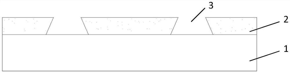
[0070] 5) Etching the hard compound layer 2 with plasma, adjusting the angle between the plasma and the hard compound layer 2 to be 70° to form an opening 3 with a side slope of 65°;
[0071] 6) Roughen the base structure 1 exposed by the opening 3 under the condition of cleaning the remaining photoresist on t...
Embodiment 2
[0077] A method for manufacturing a metal electrode of an LED device, comprising the steps of:
[0078] 1) Provide Micro-LED chips as the basic structure 1;
[0079] 2) Grinding the upper surface of the LED chip to a roughness of 0.2 nm by chemical mechanical polishing;
[0080] 3) Using CVD to grow 2000 Å on the upper surface of the above-mentioned LED chip thick hard compound layer 2;
[0081] 4) Coating photoresist on the surface of the hard compound layer 2, and baking at 95°C to form a photoresist layer 4 with a thickness of 2um, and then using a mask to expose and develop to form a photoresist opening with an opening 3 width of 5um 5;
[0082] 5) Etching the hard compound layer 2 with plasma, adjusting the angle between the plasma and the hard compound layer 2 to be 70° to form an opening 3 with a side slope of 65°;
[0083]6) Roughen the base structure 1 exposed by the opening 3 under the condition of cleaning the remaining photoresist on the surface, so that the...
Embodiment 3
[0089] A method for manufacturing a metal electrode of an LED device, comprising the steps of:
[0090] 1) Provide Mini LCD LED chips as the basic structure 1;
[0091] 2) Grinding the upper surface of the LED chip to a roughness of 0.3 nm by chemical mechanical polishing;
[0092] 3) Using CVD to grow 3000 Å on the upper surface of the above-mentioned LED chip thick hard compound layer 2;
[0093] 4) Coating photoresist on the surface of the hard compound layer 2, and baking at 95° C. to form a photoresist layer 4 with a thickness of 3 um, and then using a mask to expose and develop to form a photoresist opening 3 with a width of 10 um 5;
[0094] 5) Etching the hard compound layer 2 with plasma, adjusting the angle between the plasma and the hard compound layer 2 to be 70° to form an opening 3 with a side slope of 65°;
[0095] 6) Roughen the base structure 1 exposed by the opening 3 under the condition of cleaning the remaining photoresist on the surface, so that the...
PUM
| Property | Measurement | Unit |
|---|---|---|
| Thickness | aaaaa | aaaaa |
| Thickness | aaaaa | aaaaa |
| Thickness | aaaaa | aaaaa |
Abstract
Description
Claims
Application Information
 - R&D Engineer
- R&D Manager
- IP Professional
- Industry Leading Data Capabilities
- Powerful AI technology
- Patent DNA Extraction
Browse by: Latest US Patents, China's latest patents, Technical Efficacy Thesaurus, Application Domain, Technology Topic.
© 2024 PatSnap. All rights reserved.Legal|Privacy policy|Modern Slavery Act Transparency Statement|Sitemap