Composite film sensor for measuring heat flux density and pressure and preparation method thereof
A thin-film sensor and heat flux technology, applied in the direction of measuring force, measuring heat, measuring devices, etc., can solve the problems of time-consuming disassembly, transformation and installation, the inability to guarantee simultaneous output of two parameters, and different response times to achieve output The effect of good signal effect, increased air expansion, and simple signal collection
- Summary
- Abstract
- Description
- Claims
- Application Information
AI Technical Summary
Problems solved by technology
Method used
Image
Examples
Embodiment 1
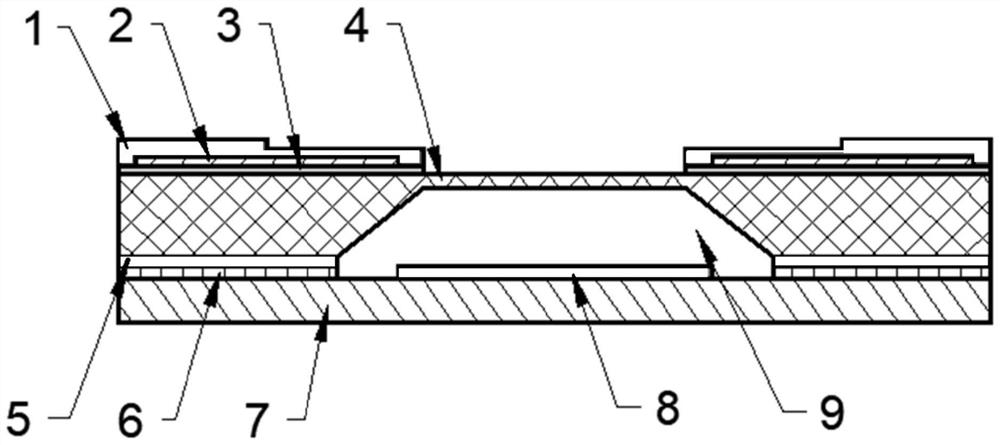
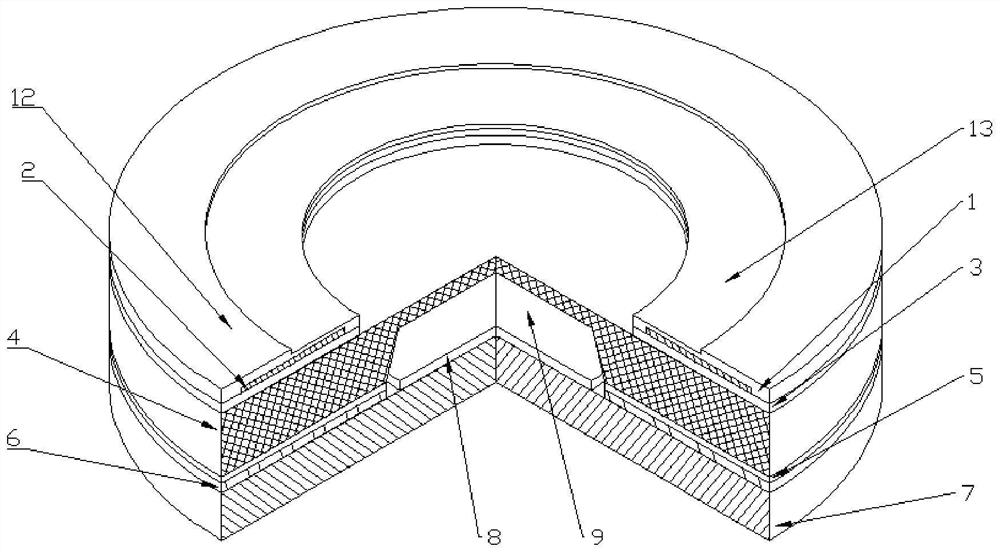
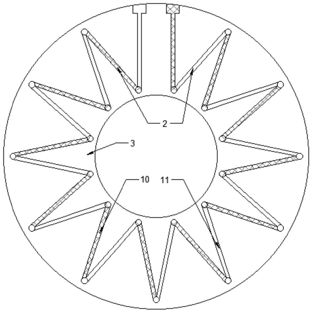
[0038] refer to figure 1 , a composite film sensor for measuring heat flux density and pressure, including a capacitive film pressure sensing part and a heat flux sensing part. Among them, the capacitive thin-film pressure sensing part includes a doped silicon substrate 4, a dielectric insulating layer 5, a polysilicon layer 6 and a pressure-sensitive substrate 7 are sequentially deposited below the doped silicon substrate 4, and the pressure-sensitive substrate 7 and the doped silicon There is a vacuum sealed cavity 9 between the substrates 4 , and the pressure sensitive substrate 7 is provided with a capacitor lower plate 8 , and the capacitor lower plate 8 is located in the vacuum sealed cavity 9 . Above the capacitive film pressure sensing part, there are thermopile layer base 3, thermopile layer 2 and thermal resistance layer 1 arranged in sequence from bottom to top, and thermopile layer base 3, thermopile layer 2 and thermal resistance layer 1 form a heat flux density s...
Embodiment 2
[0049] A method for preparing a composite thin film sensor for measuring heat flux density and pressure, the main structural parameters of which are:
[0050] The thickness of the upper plate of the capacitor is 8.5 μm to 15 μm, the diameter is 5 mm to 7.5 mm, and the height of the vacuum sealed chamber 9 is 7 μm to 10 μm. The line width of the thermocouple material deposition is less than 150 μm, the line length is 7 mm to 15 mm, and the thickness is 1 μm to 2 μm to ensure the continuity of the thermocouple.
[0051] Combine below Figure 4 The preparation method of the present invention is described in detail:
[0052] Step 1. Take an n-type single-crystal silicon wafer 14, and clean the single-crystal silicon wafer 14 with a standard cleaning method.
[0053] Step 2. Deposit an oxide layer on the single crystal silicon wafer 14 and perform photolithography. The oxide layer is used as a chemical barrier layer, and wet anisotropic silicon etching is performed with KOH solu...
PUM
| Property | Measurement | Unit |
|---|---|---|
| thickness | aaaaa | aaaaa |
| diameter | aaaaa | aaaaa |
| width | aaaaa | aaaaa |
Abstract
Description
Claims
Application Information
 - R&D Engineer
- R&D Manager
- IP Professional
- Industry Leading Data Capabilities
- Powerful AI technology
- Patent DNA Extraction
Browse by: Latest US Patents, China's latest patents, Technical Efficacy Thesaurus, Application Domain, Technology Topic, Popular Technical Reports.
© 2024 PatSnap. All rights reserved.Legal|Privacy policy|Modern Slavery Act Transparency Statement|Sitemap|About US| Contact US: help@patsnap.com


