Novel radiation refrigeration device based on broadband absorber with metasurface
A technology of radiative cooling and metasurface, applied in instruments, optical components, optics, etc., can solve the problems of unstable cooling effect, low cooling effect, easy damage of film, etc., achieve easy mass production of large area, reduce preparation cost, The effect of improving production efficiency
- Summary
- Abstract
- Description
- Claims
- Application Information
AI Technical Summary
Problems solved by technology
Method used
Image
Examples
Embodiment 1
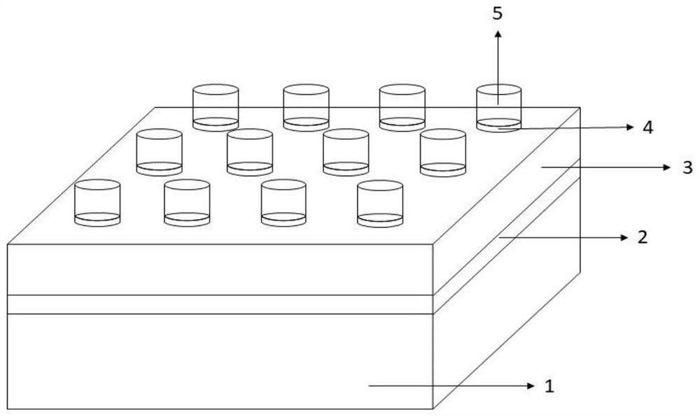
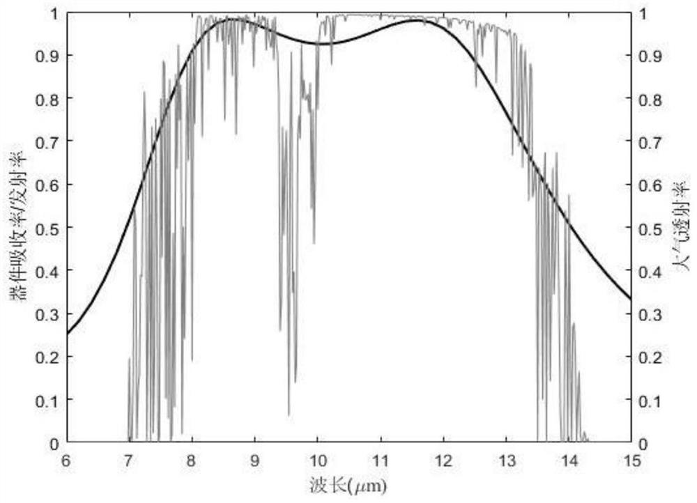
[0034] Under the incidence of TE wave, the material used in the reflective film with uniform optical thickness in the absorber is metal titanium with a thickness of 100nm, and the intermediate dielectric layer covering the bottom metal film is germanium with a thickness of 480nm. The periodic array is formed by stacking plasmonic metal titanium discs and dielectric germanium cylinders with the same radius. The period of 1 μm is spread out in a two-dimensional planar tetragonal lattice on the upper surface of the intermediate dielectric layer. The thickness of the titanium disc is 20nm, and the germanium cylinder The thickness is 500nm. The spectra of the above absorbers are shown in figure 2 As shown by the black solid line, it can be seen that it basically coincides with the atmospheric infrared transparent window (gray solid line), and the average absorption rate in the 8-13 μm working band is 0.94.
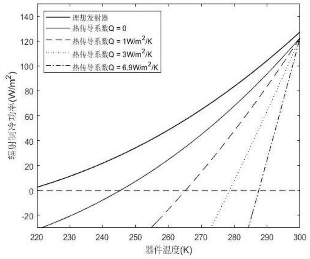
[0035] The radiation cooling power of the absorber of embodiment 1 under...
Embodiment 2
[0037]On the basis of Embodiment 1, modify the thickness of the intermediate germanium dielectric layer to 400nm, 430nm, 450nm, 480nm, and 500nm respectively. The spectra of the above absorbers are shown in Figure 4 It can be seen that modifying the thickness of the intermediate dielectric layer of the absorber will affect the absorptivity, but within a certain range of modification, the absorptivity has little effect, and the device can still maintain a high broadband average absorptivity, thereby reducing the Accuracy requirements for absorber preparation.
Embodiment 3
[0039] On the basis of Example 1, modify the period of the plasmonic titanium metal disc and the dielectric germanium cylinder array to be 0.8 μm, 1 μm, 1.2 μm, and 1.4 μm, respectively. The spectra of the above absorbers are shown in Figure 5 As shown, it can be seen that if the period is too large, the absorption bandwidth will be reduced, so that it is impossible to maintain a high average absorption rate in the working band of 8 μm to 13 μm, and if the period is too small, the absorption rate in the working band will be reduced, which will also reduce the average absorption rate. . However, the array period changes within a certain range, and the device can still maintain a high absorption rate in the working band.
PUM
| Property | Measurement | Unit |
|---|---|---|
| thickness | aaaaa | aaaaa |
| thickness | aaaaa | aaaaa |
| thickness | aaaaa | aaaaa |
Abstract
Description
Claims
Application Information
 - R&D
- Intellectual Property
- Life Sciences
- Materials
- Tech Scout
- Unparalleled Data Quality
- Higher Quality Content
- 60% Fewer Hallucinations
Browse by: Latest US Patents, China's latest patents, Technical Efficacy Thesaurus, Application Domain, Technology Topic, Popular Technical Reports.
© 2025 PatSnap. All rights reserved.Legal|Privacy policy|Modern Slavery Act Transparency Statement|Sitemap|About US| Contact US: help@patsnap.com


