Wafer uniform glue baking machine

A technology for baking machines and wafers, applied in conveyors, conveyor objects, conveyor control devices, etc., can solve the problems of slow speed, low efficiency, and the thickness and width of the glue are not fixed, so as to improve the degree of automation, Guarantee baking quality and improve work efficiency

Pending Publication Date: 2022-03-01
苏州康沃斯智能装备有限公司
View PDF0 Cites 3 Cited by
  • Summary
  • Abstract
  • Description
  • Claims
  • Application Information

AI Technical Summary

Problems solved by technology

[0003] At present, in the photoresist coating process, the wafer is generally put into a special coating machine, and the spin coating method is used to complete it. In the process of wafer packaging coating, the wafer needs to be heat treated. , drying, and even some manufacturers’ wafer gluing is completely manual. The periphery of the wafer that needs gluing is manually applied with a small script brush. Manual gluing will lead to the thickness of the glue coating and the coverage area. Unevenness, slow speed, and low efficiency seriously affect the production efficiency of semiconductor devices, and the thickness and width of the glue coating are not fixed. The uniformity of the thickness of the photolithography glue coating will directly affect the photolithography effect. With the fluctuation of the glue thickness, The photoresist line width will also fluctuate accordingly. To ensure the stability of the photoresist pattern, it is necessary to improve the uniformity of the thickness of the photoresist. At the same time, the effect of heat treatment has a great influence on the uniformity of the final photoresist coating. Therefore, not only To improve the uniformity of gluing and the quality of baking, it is also necessary to improve the efficiency of wafer gluing and drying

Method used


Image

  • Wafer uniform glue baking machine
  • Wafer uniform glue baking machine
  • Wafer uniform glue baking machine

Examples


Embodiment Construction

[0034] The following will clearly and completely describe the technical solutions in the embodiments of the present invention with reference to the accompanying drawings in the embodiments of the present invention. Obviously, the described embodiments are only some, not all, embodiments of the present invention. Based on the embodiments of the present invention, all other embodiments obtained by persons of ordinary skill in the art without making creative efforts belong to the protection scope of the present invention.

[0035] see figure 1 —13, the present invention provides a technical solution:

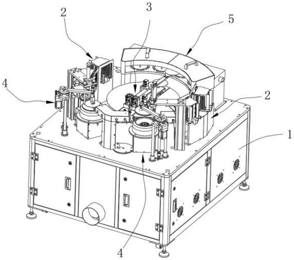
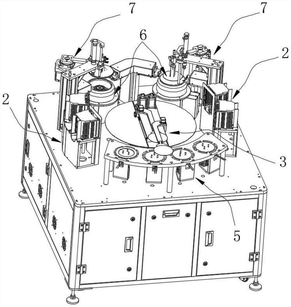
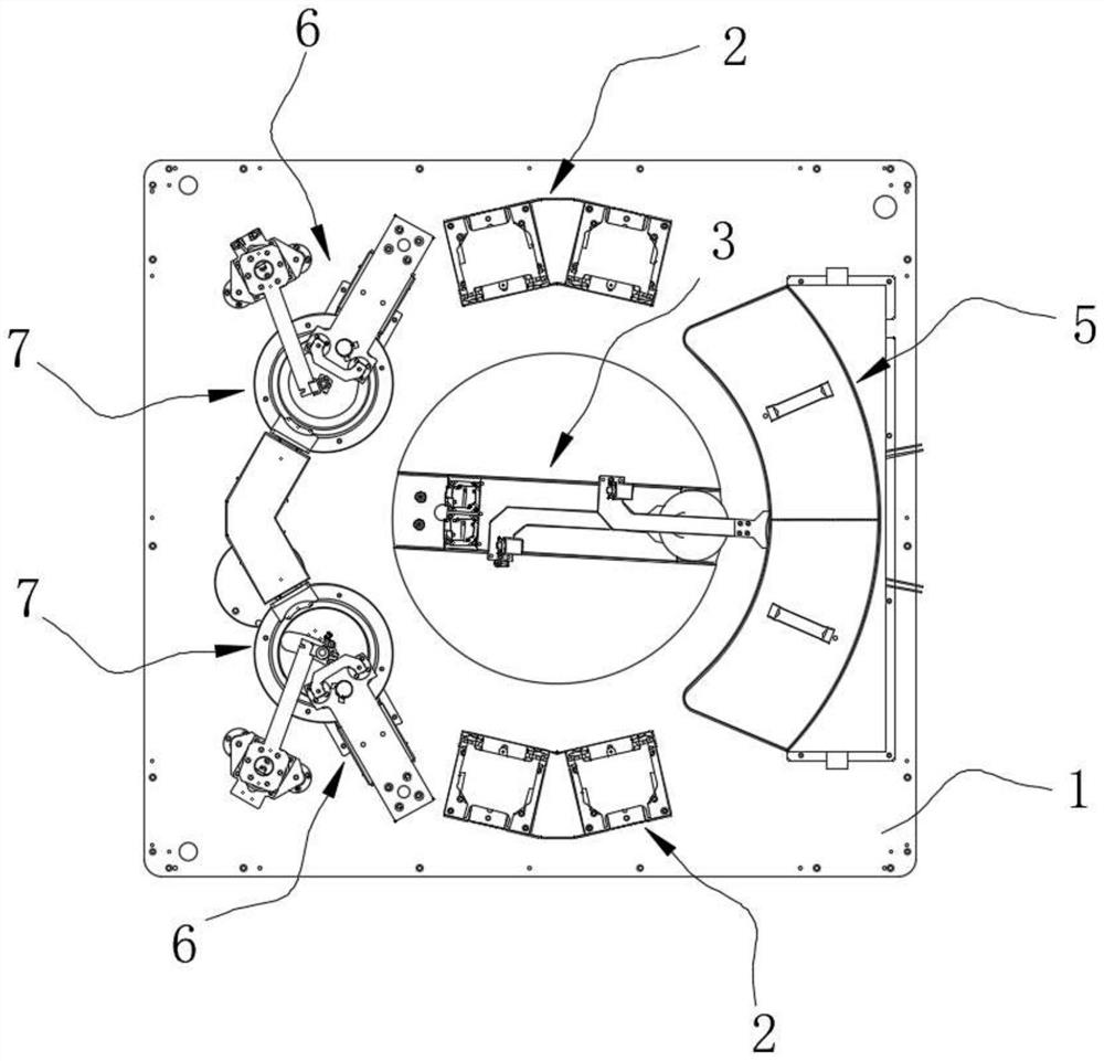
[0036] A wafer coating baking machine, which includes a frame 1, the upper surface of the frame 1 is provided with a receiving and feeding rack 2, a manipulator 3, a coating module 4 and a baking table 5, and the manipulator 3 is arranged on the frame 1 At the center of the center, the receiving and feeding rack 2, the rubber uniform module 4 and the baking table 5 are arranged on...


PUM


Abstract

A wafer uniform glue baking machine disclosed by the present invention comprises a rack, the upper surface of the rack is provided with a material receiving and supplying rack, a manipulator, a uniform glue module and a baking table, the material receiving and supplying rack is used for placing a wafer, the uniform glue module comprises a gluing mechanism and a uniform glue spin-drying mechanism, the gluing mechanism is used for gluing the wafer, the uniform glue spin-drying mechanism is used for uniformly smearing glue on the wafer, and the baking table is used for baking the wafer. The baking table is used for drying the glued wafer; according to the invention, after the wafer is taken out from the material receiving and supplying frame through the manipulator, the wafer is placed on the glue uniformizing module for glue coating and uniform smearing, the wafer is transferred to the baking table after glue coating is completed, and finally the dried wafer is placed in the material receiving and supplying frame, so that automatic glue coating, glue uniformizing and baking of the wafer are realized, the automation degree of the equipment is improved, and the production efficiency is improved. According to the photoresist coating device, the coating uniformity is guaranteed, meanwhile, the thickness of the photoresist on the surface meets the requirement, then the photoresist is dried through the baking table, the baking quality is guaranteed, and the photoresist coating uniformity is further improved.

Description

technical field [0001] The invention relates to the technical field of wafer processing, in particular to a wafer coating baking machine. Background technique [0002] In the process of semiconductor preparation and packaging, the photolithography process is mainly used. Among them, the photolithography process refers to the process of photoresist coating, exposure and development on the substrate, and the transfer of the designed pattern on the photolithography mask plate to the substrate. The process in the film layer on the surface of the substrate, in the photoresist coating process, the photoresist film layer is formed by coating the photoresist solution on the substrate surface and heating the coated photoresist solution, and then A prescribed pattern structure is formed in the photoresist layer on the surface of the substrate through an exposure and development process. [0003] At present, in the photoresist coating process, the wafer is generally put into a special...

Claims


Application Information

Patent Timeline
Patent Type & Authority Applications(China)
IPC IPC(8): B05C5/02B05C9/14B05C11/10B05C13/02B05D3/02B65G43/08B65G47/90
CPCB05C5/02B05C11/10B05C13/02B05C9/14B05D3/0254B65G47/902B65G47/905B65G43/08B65G2203/044
Inventor 高波
Owner 苏州康沃斯智能装备有限公司
Why Eureka
Try Eureka