Lateral double-diffused metal oxide semiconductor field effect transistor and manufacturing method thereof

An oxide semiconductor and lateral double-diffusion technology, which is applied in semiconductor/solid-state device manufacturing, semiconductor devices, electrical components, etc., can solve the problems of increasing LDMOSFET chip area and on-resistance, and LDMOSFET cannot meet the application requirements, so as to reduce the Effect of surface electric field, high breakdown voltage, and improvement of breakdown voltage

Inactive Publication Date: 2022-01-21
BEIJING CHIP IDENTIFICATION TECH CO LTD +2
View PDF3 Cites 9 Cited by
  • Summary
  • Abstract
  • Description
  • Claims
  • Application Information

AI Technical Summary

Problems solved by technology

Generally, the breakdown voltage can be increased by increasing the channel length and the length of the drift region, but this will increase the area and on-resistance of the LDMOSFET chip
Due to the contradictory relationship between high breakdown voltage and low characteristic on-resistance, existing LDMOSFETs cannot meet the requirements of the application

Method used


Image

  • Lateral double-diffused metal oxide semiconductor field effect transistor and manufacturing method thereof
  • Lateral double-diffused metal oxide semiconductor field effect transistor and manufacturing method thereof
  • Lateral double-diffused metal oxide semiconductor field effect transistor and manufacturing method thereof

Examples


Embodiment Construction

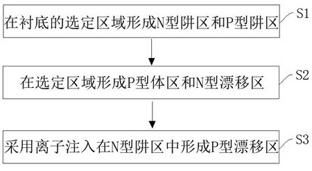
[0032] Specific embodiments of the present invention will be described in detail below in conjunction with the accompanying drawings. It should be understood that the specific embodiments described here are only used to illustrate and explain the present invention, and are not intended to limit the present invention.

[0033] figure 1 It is a schematic structural diagram of a lateral double-diffused metal-oxide-semiconductor field effect transistor provided in an embodiment of the present invention. Such as figure 1 As shown, the lateral double diffused metal oxide semiconductor field effect transistor (hereinafter referred to as LDMOSFET) of this embodiment includes a substrate 100, a gate region 101, a source region 102, a drain region 103, a shallow trench isolation region 111, a P body region 104 , N-type well region 106 , P-type well region ( 107 a / 107 b ) and N-type drift region ( 105 a / 105 b ) located on the substrate 100 . The LDMOSFET of this embodiment further...


PUM


Abstract

The invention relates to the technical field of semiconductors, and provides a lateral double-diffused metal oxide semiconductor field effect transistor and a manufacturing method thereof. The lateral double-diffused metal oxide semiconductor field effect transistor comprises a substrate, a gate region, a source region, a drain region, a P-type body region, and an N-type well region, a P-type well region and an N-type drift region which are positioned on the substrate, and further comprises a P-type drift region formed by ion implantation, wherein the P-type drift region is located in the N-type well region, and a preset distance exists between the P-type drift region and the P-type body region. According to the invention, the P-type drift region is added in the N-type well region, the contact surface of the P-type drift region and the N-type well region forms a PN junction, and the P-type drift region and the N-type drift region form a dual RESURF structure, so that the surface electric field of the device is reduced, higher breakdown voltage can be borne, and lower on-resistance can be maintained.

Description

technical field [0001] The invention relates to the field of semiconductor technology, in particular to a lateral double-diffused metal oxide semiconductor field effect transistor and a method for manufacturing the lateral double-diffused metal oxide semiconductor field effect transistor. Background technique [0002] Double-diffused metal oxide semiconductor field effect transistor (Double-diffused MOS, referred to as DMOS) has the characteristics of high withstand voltage, low power consumption, high current driving capability, etc., and is widely used in power management circuits. There are two main types of double diffused metal oxide semiconductor field effect transistors, vertical double diffused metal oxide semiconductor field effect transistor (Vertical Double-diffused MOSFET, referred to as VDMOSFET) and lateral double diffused metal oxide semiconductor field effect transistor (LateralDouble-diffused MOSFET) MOSFET, referred to as LDMOSFET). [0003] For LDMOSFET, ...

Claims


Application Information

Patent Timeline
Patent Type & Authority Applications(China)
IPC IPC(8): H01L29/06H01L29/78H01L21/336
CPCH01L29/7816H01L29/66681H01L29/0684H01L29/0623H01L29/0634
Inventor 余山赵东艳王于波陈燕宁付振刘芳王凯吴波邓永峰刘倩倩郁文
Owner BEIJING CHIP IDENTIFICATION TECH CO LTD
Why Eureka
Try Eureka