Production method for enhanced GaN transistor

A manufacturing method and technology of gallium nitride, which are applied in semiconductor/solid-state device manufacturing, semiconductor devices, electrical components, etc., can solve the problems of small on-resistance and high withstand voltage of gallium nitride transistors, and achieve reduced on-resistance, The effect of reducing the surface electric field and improving the withstand voltage

Inactive Publication Date: 2017-10-03
PEKING UNIV +2
View PDF3 Cites 2 Cited by
  • Summary
  • Abstract
  • Description
  • Claims
  • Application Information

AI Technical Summary

Problems solved by technology

[0004] The larger the on-resistance of the gallium nitride transistor, the greater the withstand voltage, but usually those skilled in the art hope that the on-resistance of the gallium nitride transistor is small and the withstand voltage is as large as possible, but the existing manufacturing process is difficult to meet GaN transistors have low on-resistance and high withstand voltage

Method used


Image

  • Production method for enhanced GaN transistor
  • Production method for enhanced GaN transistor
  • Production method for enhanced GaN transistor

Examples


Embodiment Construction

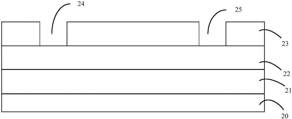
[0023] figure 1 The flow chart of the fabrication method of the enhancement mode gallium nitride transistor provided by the embodiment of the present invention. In order to describe the method in this embodiment clearly and systematically, Figure 2-Figure 8 A schematic cross-sectional view of an enhancement-mode gallium nitride transistor during the implementation of the method of the embodiment of the present invention, as shown in figure 1 As shown, the method includes:

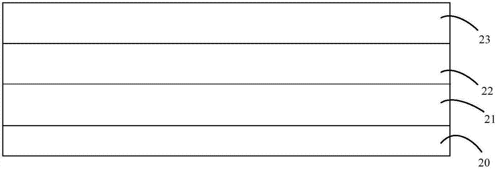
[0024] Step S101, sequentially growing a phosphorus-doped GaN dielectric layer, an aluminum gallium nitride AlGaN dielectric layer, and a silicon nitride Si3N4 dielectric layer on the surface of a silicon substrate;

[0025] Such as figure 2 As shown, a phosphorus-doped GaN dielectric layer, an aluminum gallium nitride AlGaN dielectric layer and a silicon nitride Si3N4 dielectric layer are sequentially grown on the surface of a silicon substrate, and the schematic cross-sectional view after performing ...


PUM


Abstract

The embodiment of the invention provides a production method for an enhanced GaN transistor. The method comprises the steps of growing a phosphorus-doped GaN dielectric layer, an AlGaN dielectric layer and an Si3N4 dielectric layer on the surface of a silicon substrate in sequence; etching the Si3N4 dielectric layer; depositing metal layers on the upper surfaces of the exposed AlGaN dielectric layer and the residual Si3N4 dielectric layer; carrying out dry etching downward along a predetermined area of the surface of the exposed Si3N4 dielectric layer; and depositing an SiO2 dielectric layer in a gate contact hole as gate dielectric. According to the embodiment of the invention, the phosphorus-doped GaN dielectric layer is grown on the surface of the silicon substrate and a surface electric field of the enhanced GaN transistor is reduced, so the voltage resistance is improved; and moreover, phosphorus is doped in a gate of the enhanced GaN transistor and the composition of electrons and holes exists, so the on resistance is reduced, and a technology demand that the on resistance of the GaN transistor is relatively low and the voltage resistance is relatively high is realized.

Description

technical field [0001] Embodiments of the present invention relate to the field of semiconductors, and in particular, to a method for manufacturing an enhancement mode gallium nitride transistor. Background technique [0002] Power devices featuring low power consumption and high speed have recently attracted a lot of attention as the need for efficient and complete power conversion circuits and systems has increased. Gallium nitride GaN is the third-generation wide-bandgap semiconductor material. Due to its large bandgap (3.4eV), high electron saturation rate (2e7cm / s), and high breakdown electric field (1e10--3e10V / cm), it is relatively High thermal conductivity, corrosion resistance and radiation resistance, have strong advantages in high pressure, high frequency, high temperature, high power and anti-irradiation environmental conditions, it is considered to be the best choice for researching short-wave optoelectronic devices and high-voltage, high-frequency and high-powe...

Claims


Application Information

Patent Timeline
Patent Type & Authority Applications(China)
IPC IPC(8): H01L21/335H01L21/28H01L21/321H01L29/06
CPCH01L29/66462H01L21/32155H01L29/0623H01L29/42372
Inventor 刘美华孙辉林信南陈建国
Owner PEKING UNIV
Why Eureka
Try Eureka