
Optical fiber array connecting device and manufacturing method thereof

An optical fiber array and connecting device technology, which is applied in the field of optical fiber array connecting device and its production, can solve the problems such as the large volume of the optical connection interface, the difficulty in meeting the required size of the inter-chip connection, the number of optical fibers, and the inability of the optical fiber density to meet the optical connection. , to avoid excessive volume, increase the number of optical fibers, and improve the density of optical fibers

Pending Publication Date: 2021-12-31
T&S COMM
View PDF7 Cites 2 Cited by
  • Summary
  • Abstract
  • Description
  • Claims
  • Application Information

AI Technical Summary

Problems solved by technology

However, the use of V-groove makes the optical connection interface too large, and the fiber density cannot meet the requirements of optical connection.
For example, the size of the current micro-LED can reach 2um*2um, but the size of the V-groove itself and the spacing requirements between the V-grooves are difficult to meet the size and the number of optical fibers required for the connection between chips.

Method used


Image

  • Optical fiber array connecting device and manufacturing method thereof
  • Optical fiber array connecting device and manufacturing method thereof
  • Optical fiber array connecting device and manufacturing method thereof

Examples


Embodiment Construction

[0032] Embodiments of the present invention will be described in detail below. It should be emphasized that the following description is only exemplary and not intended to limit the scope of the invention and its application.

[0033] It should be noted that when an element is referred to as being “fixed” or “disposed on” another element, it may be directly on the other element or be indirectly on the other element. When an element is referred to as being "connected to" another element, it can be directly connected to the other element or indirectly connected to the other element. In addition, the connection can be used for fixation as well as for coupling or communication.

[0034] It is to be understood that the terms "length", "width", "top", "bottom", "front", "rear", "left", "right", "vertical", "horizontal", "top" , "bottom", "inner", "outer" and other indicated orientations or positional relationships are based on the orientations or positional relationships shown in ...


PUM


Abstract

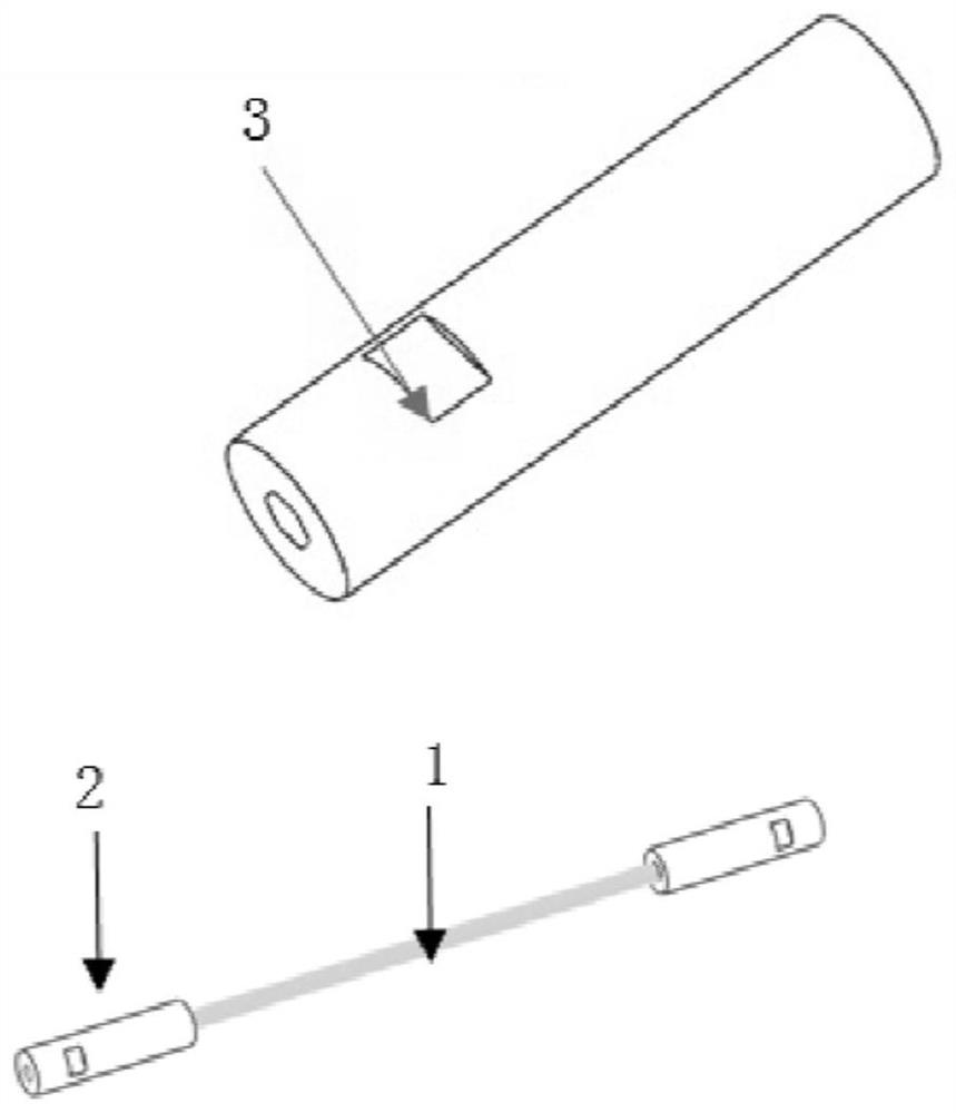
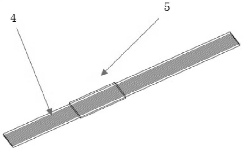
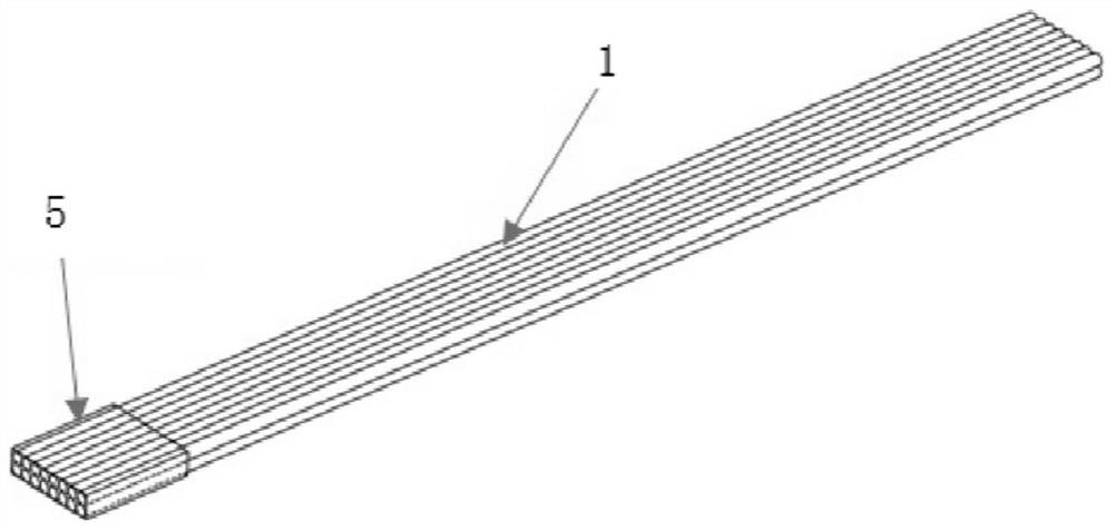
The invention discloses an optical fiber array connecting device and a manufacturing method thereof. The connecting device comprises an optical fiber connector and an optical fiber array, the optical fiber array comprises a plurality of optical fibers which are arranged in order, each optical fiber is tightly attached to the optical fibers around the optical fiber in the mode that the outer surfaces of the optical fibers are tangent, and the two ends or any one end of the optical fiber array is arranged in the optical fiber connector, and the overall shape of the optical fiber array is bound and positioned by the inner surface of the optical fiber connector; a positioning structure is arranged on the optical fiber connector and is used for being matched with a corresponding positioning structure on an interface of to-be-connected equipment; the positioning structure and the arrangement of the optical fibers have a determined position relationship so as to maintain the overall position of the optical fiber array relative to the interface of the to-be-connected equipment, and light emitted by the to-be-connected equipment can be coupled into the optical fibers. According to the invention, the optical fiber array with high-density optical fiber distribution can be realized with a small size.

Description

technical field [0001] The invention relates to an optical communication device, in particular to an optical fiber array connection device and a manufacturing method thereof. Background technique [0002] With the continuous reduction of transistor feature size, electrical interconnection faces limitations such as large signal delay, small transmission bandwidth, large signal crosstalk, high power consumption, difficult processing, and high cost, and the speed of increasing integration slows down or even stagnates. [0003] The structure of metal interconnection in the current circuit is becoming more and more complex, and interconnection technology is developing towards high-speed and high-density integration to meet the current needs of large-capacity and high-speed transmission. With the continuous reduction of transistor feature size Small, electrical interconnection faces limitations such as large signal delay, small transmission bandwidth, large signal crosstalk, high ...

Claims


Application Information

Patent Timeline
IPC IPC(8): G02B6/38G02B6/40
CPCG02B6/3889G02B6/40
Inventor 谢峥张凯波扈士超徐东杨智敏
Owner T&S COMM
Learn More