Micro-LED optical information sensing and storage unit, photonic integrated chip, array and preparation method

A technology of storage unit and storage array, applied in information storage, static memory, digital memory information, etc., can solve the problems of data transmission energy and efficiency loss, complex integration process, low integration degree, etc., to improve signal processing efficiency, simplify Circuit structure, the effect of high integration

Active Publication Date: 2021-12-03
HUNAN UNIV
View PDF9 Cites 0 Cited by
  • Summary
  • Abstract
  • Description
  • Claims
  • Application Information

AI Technical Summary

Problems solved by technology

[0003] Silicon material has an indirect band gap and low luminous efficiency, which will affect the overall energy efficiency when used as a signal source in photonic integrated chips
In the prior art, the photoelectric sensor and the memory are connected by copper wires, the signal transmission is limited by the bandwidth, and the application in the future big data and long-distance real-time image display is limited
In addition, the current photonic chips have high requirements on the number and performance of sensing units and storage units. The existing technology separates each unit from the physical level, which not only has low integration and complex integration process, but also causes energy and energy consumption in data transmission. Huge loss of efficiency, limited in application and cost

Method used


Image

  • Micro-LED optical information sensing and storage unit, photonic integrated chip, array and preparation method
  • Micro-LED optical information sensing and storage unit, photonic integrated chip, array and preparation method
  • Micro-LED optical information sensing and storage unit, photonic integrated chip, array and preparation method

Examples


Embodiment 1

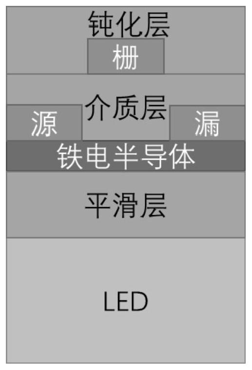
[0042] This embodiment provides an information sensing and storage unit of a photonic integrated chip, such as figure 1 As shown, it includes Micro-LEDs, smoothing layers, ferroelectric semiconductors, dielectric layers and passivation layers that are sequentially aligned and stacked from bottom to top, and also includes source, drain and gate. The source and drain They are respectively embedded on both sides of the bottom of the dielectric layer and are in contact with the ferroelectric semiconductor, and the gate is embedded in the bottom of the passivation layer and located in the middle above the dielectric layer.

[0043]Among them, the microLED uses III-V compound light-emitting materials, which has the advantages of high brightness and high integration, and is an excellent choice for on-chip light sources. The substrate of the microLED can be a rigid substrate such as sapphire, silicon, silicon carbide, gallium nitride, or a flexible substrate such as a polymer such as ...

Embodiment 2

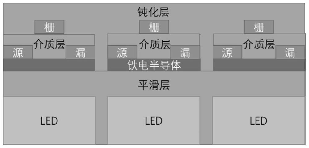
[0050] This embodiment provides a photonic integrated chip, including an array composed of several information sensing and storage units of the photonic integrated chip described in Embodiment 1, such as figure 2 shown.

Embodiment 3

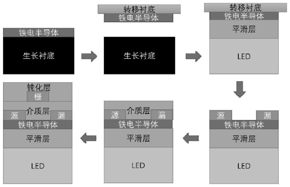
[0052] This embodiment provides a preparation method for the information sensing and storage unit of the photonic integrated chip described in Embodiment 1, refer to image 3 shown, including the following steps:

[0053] Step A1, obtaining a micro-LED on a silicon substrate.

[0054] The substrate of the microLED can be a steel base material such as sapphire, silicon, silicon carbide, gallium nitride, etc., or a flexible base such as a high molecular polymer such as PET. The LED epitaxial layer includes P-type semiconductors, quantum wells, The N-type semiconductor and the semiconductor material of the buffer layer between the substrate and the semiconductor material are mainly compounds of Group III and V materials such as GaN, InGaN, and AlGaN. Evaporated electrodes form the contacts of the micro-LED, and the electrode materials can be Au, Ag, Cu, ITO, etc.

[0055] Step A2, deposit a smooth layer on the micro-LED, the material can be SiO x , SiN x , AlO x etc., and th...


PUM


Abstract

The invention discloses a Micro-LED optical information sensing and storage unit, a photonic integrated chip, an array and a preparation method. The information sensing and storage unit of the photonic integrated chip comprises a Micro-LED, a smooth layer, a ferroelectric semiconductor, a dielectric layer and a passivation layer which are sequentially aligned with one another and superposed from bottom to top; and the information sensing and storage unit also comprises a source electrode, a drain electrode and a grid electrode, wherein the source electrode and the drain electrode are respectively embedded into two sides of the bottom of the dielectric layer and are in contact with the ferroelectric semiconductor, and the grid electrode is embedded into the bottom of the passivation layer and is located at the middle position above the dielectric layer. According to the micro-LED optical information sensing and storage unit, the photonic integrated chip, the array and the preparation method of the invention, synchronous sensing and storage of optical information can be realized, the signal processing efficiency is improved, and the circuit structure is simplified. The micro-LED optical information sensing and storage unit has important application prospects in the fields of photon chips and image recognition in the future.

Description

technical field [0001] The invention belongs to the technical field of optoelectronic devices and integration, and in particular relates to a Micro-LED optical information sensing and storage unit, a photonic integrated chip, an array and a preparation method. Background technique [0002] Photonic integrated chips use photons as carriers to realize information transmission and processing. Compared with current integrated circuits that use electrons as transmission signals, photons can increase the speed of signal transmission and reduce the use of interconnected copper wires, thereby reducing power consumption. It is the future The mainstream direction of information technology development. The photonic integrated chip is composed of multiple optical-related functional units and devices, on-chip light source, optical waveguide, optical modulator, optical detector, storage unit, computing unit, etc., which mainly realize the propagation of photons on the chip, as well as the...

Claims


Application Information

Patent Timeline
Patent Type & Authority Applications(China)
IPC IPC(8): H01L27/15G11C11/22
CPCH01L27/15H01L27/156G11C11/22Y02P70/50
Inventor 潘安练李晟曼张成
Owner HUNAN UNIV
Why Eureka
Try Eureka