Quasi-optical micro-cavity-based selective absorbing coating capable of being used at 800 DEG C or above
An optical microcavity and absorption coating technology, applied in coating, metal material coating process, vacuum evaporation coating, etc., can solve the problems of difficult high absorption ratio and high temperature thermal stability, and achieve the effect of high spectral selectivity
- Summary
- Abstract
- Description
- Claims
- Application Information
AI Technical Summary
Problems solved by technology
Method used
Image
Examples
Embodiment 1
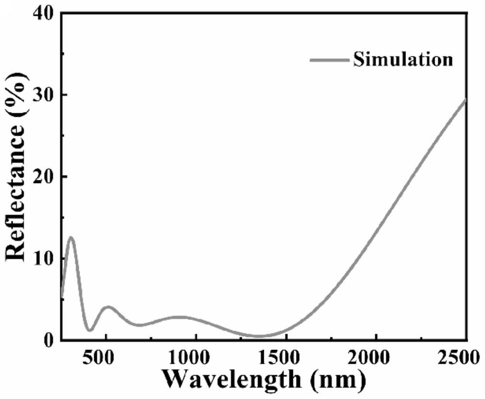
[0065] The above-mentioned preparation method is used to use ZrB in the quasi-optical microcavity structure prepared by radio frequency power sputtering under the argon environment of 0.4Pa at room temperature. 2 The material is used as the main absorbing layer of the selective absorbing coating, and the structure schematic diagram of the obtained selective absorbing coating is shown as figure 1 The specific coating parameters are shown in Table 1 below.
[0066] Table 1
[0067]
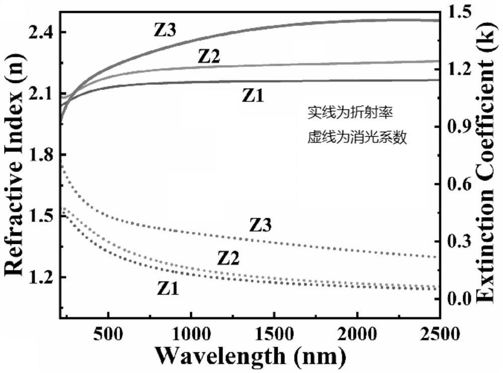
[0068] The simulated reflectance spectrum of this selective absorbing coating ZAA is as figure 2 shown. And using magnetron sputtering deposition on the Si substrate to obtain a volume ratio of 1:3 composite ceramic layer ZrB 2 -Al 2 o 3 , the volume ratio is 1:2.5 composite ceramic layer ZrB 2 -Al 2 o 3 , the volume ratio is 1:2 composite ceramic layer ZrB 2 -Al 2 o 3 , the sample numbers are Z1, Z2 and Z3 respectively, and the refractive index and extinction coefficient are tested o...
Embodiment 2
[0073] On the basis of Example 1, the ZrC material is used as the main absorbing layer of the selective absorbing coating in the quasi-optical microcavity structure prepared by radio frequency power sputtering at room temperature in an argon environment of 0.4 Pa. The selective absorbing coating of this embodiment The specific coating parameters of the layers are shown in Table 2 below.
[0074] Table 2
[0075]
[0076] The reflection spectra of the selective absorbing coating of this embodiment before and after high temperature vacuum annealing at 800°C and 900°C for 100 hours are as follows: Figure 12 As shown, the solar absorptivity and thermal emissivity under different heat treatment conditions are as Figure 13 As shown, the light-to-heat conversion efficiency diagram at different focusing magnifications is shown in Figure 14 As shown, the total efficiency of photoelectric conversion under different focusing magnifications is as follows Figure 15 shown. The ab...
PUM
| Property | Measurement | Unit |
|---|---|---|
| thickness | aaaaa | aaaaa |
| thickness | aaaaa | aaaaa |
| thickness | aaaaa | aaaaa |
Abstract
Description
Claims
Application Information
 - R&D
- Intellectual Property
- Life Sciences
- Materials
- Tech Scout
- Unparalleled Data Quality
- Higher Quality Content
- 60% Fewer Hallucinations
Browse by: Latest US Patents, China's latest patents, Technical Efficacy Thesaurus, Application Domain, Technology Topic, Popular Technical Reports.
© 2025 PatSnap. All rights reserved.Legal|Privacy policy|Modern Slavery Act Transparency Statement|Sitemap|About US| Contact US: help@patsnap.com


