
Single-photon avalanche diode, manufacturing method thereof and single-photon avalanche diode array

A technology of single-photon avalanche and production method, which is applied in the fields of final product manufacturing, sustainable manufacturing/processing, electrical components, etc., can solve the problems of reducing device detection performance, affecting photon detection efficiency, reducing device dark count rate, etc., to achieve improved The probability of avalanche generation, the effect of improving detection performance and reducing the dark count rate

Pending Publication Date: 2021-11-23
WUHAN XINXIN SEMICON MFG CO LTD
View PDF0 Cites 1 Cited by
  • Summary
  • Abstract
  • Description
  • Claims
  • Application Information

AI Technical Summary

Problems solved by technology

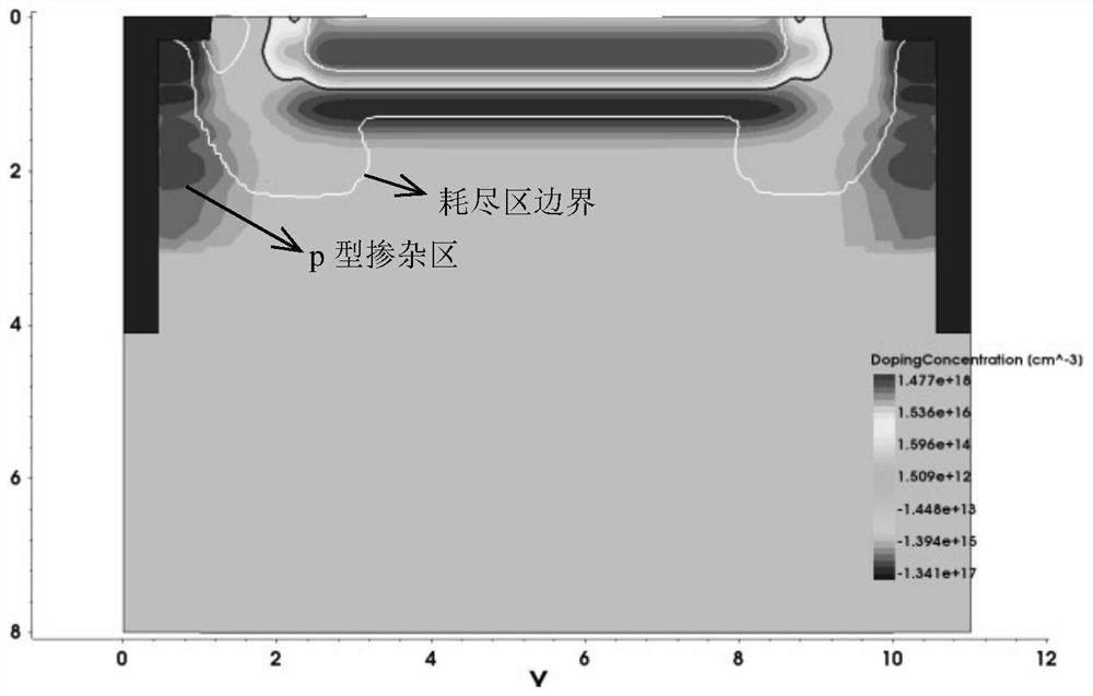
In order to reduce the dark count rate of the device, in the prior art, a p-type dopant is implanted with a certain concentration gradient next to the isolation trench used to isolate adjacent diodes to form a p-type doped region, which can effectively reduce the dark count rate caused by the isolation trench. The dark counts caused by the generated defects, however, the study found that the setting of the p-type doped region will make the depletion region of the single photon avalanche diode shrink inward, which will reduce the probability of avalanche occurrence, and then affect the photon detection efficiency. Reduced detection performance of the device

Method used


Image

  • Single-photon avalanche diode, manufacturing method thereof and single-photon avalanche diode array
  • Single-photon avalanche diode, manufacturing method thereof and single-photon avalanche diode array
  • Single-photon avalanche diode, manufacturing method thereof and single-photon avalanche diode array

Examples


Embodiment Construction

[0037] The single photon avalanche diode, its manufacturing method, and single photon avalanche diode array of the present invention will be further described in detail below with reference to the accompanying drawings and specific embodiments. The advantages and features of the present invention will become clearer from the following description. It should be understood that the drawings in the description are all in very simplified form and use imprecise scales, and are only used to facilitate and clearly assist the purpose of illustrating the embodiments of the present invention.

[0038] It should be noted that the terms "first", "second" and the like hereinafter are used to distinguish between similar elements, and are not necessarily used to describe a specific order or chronological order. It is to be understood that the terms so used are interchangeable under appropriate circumstances, for example, to enable the embodiments of the invention described herein to be opera...


PUM


Abstract

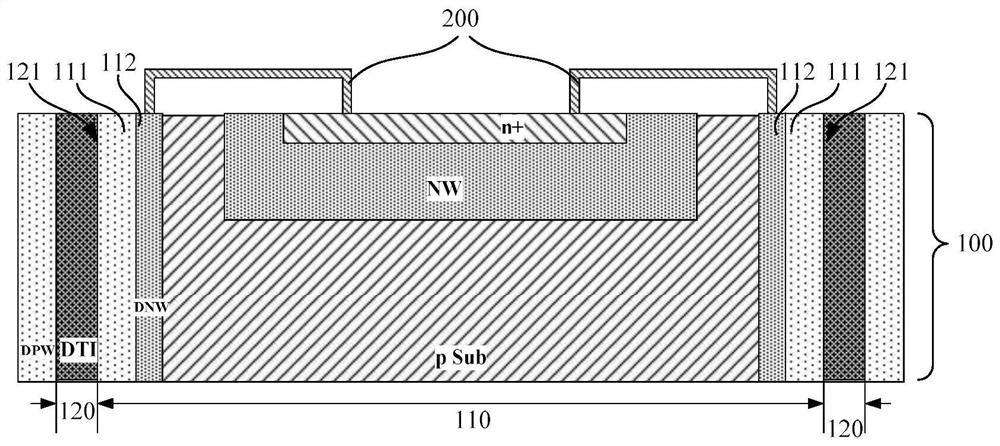
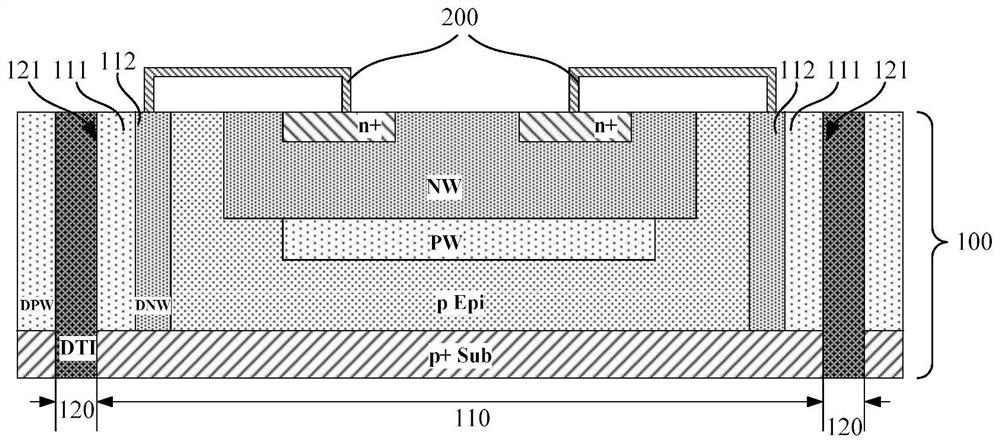
The invention relates to a single-photon avalanche diode, a manufacturing method thereof and a single-photon avalanche diode array. According to the single photon avalanche diode, a p-type doped region longitudinally extending in the thickness direction of a substrate is arranged in the edge region of an active region, and an n-type doped region longitudinally extending in the thickness direction of the substrate is further arranged on the side, away from an isolation groove, of the p-type doped region. The p-type doped region and the n-type doped region have an isolation effect on defects generated at the isolation groove, dark count caused by the defects can be effectively reduced, the n-type doped region is electrically connected with a doped region with the same doping type as the n-type doped region in the pn junction in the active region, and a depletion region shrunk due to the p-type doped region can be widened. Therefore, the dark counting rate of the single photon avalanche diode is reduced, and the photon detection efficiency of the device is not affected. The single-photon avalanche diode array comprises the single-photon avalanche diodes which are arranged in an array.

Description

technical field [0001] The invention relates to the technical field of semiconductors, in particular to a single photon avalanche diode, a manufacturing method of the single photon avalanche diode and a single photon avalanche diode array. Background technique [0002] Single photon avalanche diode, referred to as SPAD (Single Photon Avalanche Diode), is a solid-state photodetector that realizes photodetection based on the bias voltage exceeding the breakdown region of the pn junction. In single photon avalanche diodes, the pn junction is reverse biased at a voltage higher than the breakdown voltage, where the internal photoelectric effect (the emission of electrons or another type of charge carriers when a material is struck by a photon) Under the action, an avalanche current is generated. Very low signal intensities, for example down to the single photon level, can be detected with single photon avalanche diodes. Single-photon detectors based on single-photon avalanche d...

Claims


Application Information

Patent Timeline
IPC IPC(8): H01L31/107H01L31/0352H01L31/18
CPCH01L31/107H01L31/0352H01L31/18Y02P70/50
Inventor 魏丹清
Owner WUHAN XINXIN SEMICON MFG CO LTD
Learn More