


Quick Research
Generate reliable direction feasibility study reports for your R&D in just a few steps.

Technical Q&A
Discover and master advanced knowledge NOW. Basics, ideas, possibilities, all at once.

Find Solutions
As an expert in R&D theories, this can generate solutions to your technical problems instantly.

Evaluate Feasibility
Analyze your overall solution with one click, know your potential R&D risks in advance.

Monitor Landscape
Get weekly tech updates, stay abreast of the latest tech innovations and key insights.
Photoelectric nerve synaptic memristor
A neural synapse and memristor technology, applied in the field of brain-inspired computing devices, can solve the problems of light wave introduction/export methods that need to be further studied, and achieve the effect of accelerated application
- Summary
- Abstract
- Description
- Claims
- Application Information
AI Technical Summary
Problems solved by technology
Method used
Image


Examples
Embodiment 1
[0039] In embodiment 1, a kind of optoelectronic synaptic memristor, such as figure 2 As shown, the structure is from top to bottom: a silicon nitride optical waveguide layer (Si 3 N 4 ) 101, oxide isolation layer (SiO 2 ) 102, a transparent top electrode layer (ITO) 201, a two-dimensional material layer composed of molybdenum sulfide and molybdenum oxide (MoS 2 / Mo 2-x o x ) 301, graphene quantum dots modified silicon oxide porous structure layer (GQDs@PSiO x ) 401, and the bottom electrode layer (Si) 501.
[0040] Among them, the width of the optical waveguide layer (non-wedge-shaped output end part) is 5 μm, and the height is 10 μm; the inclination angle of the side of the wedge-shaped output end is 45°, and the contact surface with the top electrode is 10*10 μm 2 ; Top electrode thickness 200nm; MoS 2 / Mo 2-x o x The thickness is 10nm; the thickness of the porous structure is 100nm; the bottom electrode is 300μm.
[0041] The structure is prepared layer by layer...
Embodiment 2
[0054] In embodiment 2, such as figure 2 As shown, the structure from top to bottom is: a silicon optical waveguide layer (Si) 101 including a wedge-shaped output end 103, an oxide isolation layer (SiO 2 ) 102, transparent top electrode layer 201 (FTO), black phosphorus two-dimensional material layer (BP) 301, β-NaYF 4 :Yb 3 +,Tm 3+ / NaYF 4 Quantum dot modified silicon porous structure (β-NaYF 4 :Yb 3 +,Tm 3+ / NaYF 4 @PSi) layer 401, bottom electrode layer (Si) 501.
[0055] Among them, the width of the optical waveguide layer is 2.5 μm, and the height is 5 μm; the side of the wedge-shaped output end is inclined at an angle of 45°, and the contact surface with the top electrode is 5*5 μm 2 ; Top electrode thickness 100nm; BP thickness 3nm; porous structure thickness 150nm; bottom electrode 500μm.
[0056] The structure is prepared layer by layer on the substrate from bottom to top by electrochemical corrosion, ultrasonic dispersion, chemical vapor deposition, transfe...
Embodiment 3
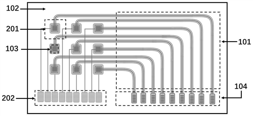
[0062] Such as figure 1 As shown, this embodiment provides a structural schematic diagram of an optoelectronic synapse array. The array structure is as follows: it includes N*M (N≥1, M≥1) photoelectric synaptic memristors, and each photoelectric synaptic memristor includes a wedge-shaped output terminal (Si 3 N 4 ) 103 silicon nitride optical waveguide layer (Si 3 N 4 ) 101, oxide isolation layer (SiO 2 ) 102, grating coupler (Si 3 N 4 ) 104, a transparent top electrode layer (ITO) 201, an external electrode (Au) 202 connecting the top electrode, and a device structure molybdenum sulfide / molybdenum oxide two-dimensional material layer (MoS 2 / Mo 2-x o x) 301, graphene quantum dots modified silicon oxide porous structure layer (GQDs@PSiO x ) 401, and the bottom electrode layer (Si) 501.
[0063] In this embodiment, an optoelectronic synapse array is obtained by integrating an optical waveguide and an optoelectronic memristor structure. Each memristor shares a common ...
PUM
| Property | Measurement | Unit |
|---|---|---|
| width | aaaaa | aaaaa |
| height | aaaaa | aaaaa |
| thickness | aaaaa | aaaaa |
Abstract
Description
Claims
Application Information
 - R&D Engineer
- R&D Manager
- IP Professional
- Industry Leading Data Capabilities
- Powerful AI technology
- Patent DNA Extraction
Browse by: Latest US Patents, China's latest patents, Technical Efficacy Thesaurus, Application Domain, Technology Topic, Popular Technical Reports.
© 2024 PatSnap. All rights reserved.Legal|Privacy policy|Modern Slavery Act Transparency Statement|Sitemap|About US| Contact US: help@patsnap.com