Suppression method for partial discharge at flange of GIS/GIL supporting insulator
A technology for supporting insulators and partial discharges, applied in insulators, processing data acquisition/processing, circuits, etc., can solve problems such as difficulty in hindering the movement of micron-level particles, and achieve high-precision manufacturing, good compatibility, and interface bonding strength high effect
- Summary
- Abstract
- Description
- Claims
- Application Information
AI Technical Summary
Problems solved by technology
Method used
Image
Examples
Embodiment 1
[0076] Example 1: 110KV disk support insulator
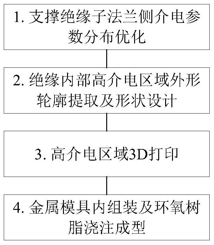
[0077] 1) Optimization of dielectric parameters of the insulator flange side
[0078] The two-dimensional axisymmetric structure of 110kV disk support insulator is like figure 2 (a) shown, in order to optimize the dielectric constant, support the root of the insulator 1 The area is a domain-based domain, and the arrow is an optimized target area Ω. 2 Ω 3 Mathematical description of the optimization problem, as design variables are designed to design a line of domain Ω 1 The dielectric constant in any mesh, the optimization target is divided into two parts, F 1 For electric field points, used to reduce optimization target area Ω 2 Ω 3 Internal electric field model. C ref1 And C ref2 F 1 The normalization parameters of the medium two optimization components make the value obtained in the initial calculation process, thereby increasing the convergence speed of the algorithm. fly 2 For gradient penalties, it is used to prevent numerical...
Embodiment 2
[0089] Example 2: 110kV Basin Support Insulator
[0090] 1) Optimization of dielectric parameters of the insulator flange side
[0091] 110kV disk support insulator to optimize the dielectric constant, support the root of the insulator 1 The area is a domain-based domain, and the arrow is an optimized target area Ω. 2 Ω 3 Mathematical description of the optimization problem is as designable to design a line of domain Ω 1 The dielectric constant in any mesh, the optimization target is divided into two parts, F 1 For electric field points, used to reduce optimization target area Ω 2 Ω 3 Internal electric field model. C ref1 And C ref2 F 1 The normalization parameters of the medium two optimization components make the value obtained in the initial calculation process, thereby increasing the convergence speed of the algorithm. fly 2 For gradient penalties, it is used to prevent numerical instability of "chessboard", improve the optimization of the manufacture of high dielectric insula...
Embodiment 3
[0102] Example 3: 550kV Basin Support Insulator
[0103] 1) Optimization of dielectric parameters of the insulator flange side
[0104] The two-dimensional axisymmetric structure of the 550kV basin support the insulator such as figure 2 (b) shown, in order to optimize the dielectric constant, support the root of the insulator 1 The area is a domain-based domain, and the arrow is an optimized target area Ω. 2 , Mathematical description of the optimization problem is 5, design variables are designed to be domain Ω 1 The dielectric constant in any mesh, the optimization target is divided into two parts, F 1 For electric field points, used to reduce optimization target area Ω 2 Ω 3 Internal electric field model. C ref Forth 1 The normalization parameters of the medium two optimization components make the value obtained in the initial calculation process, thereby increasing the convergence speed of the algorithm. fly 2 For gradient penalties, it is used to prevent numerical instability...
PUM
| Property | Measurement | Unit |
|---|---|---|
| Particle size | aaaaa | aaaaa |
Abstract
Description
Claims
Application Information
 - R&D
- Intellectual Property
- Life Sciences
- Materials
- Tech Scout
- Unparalleled Data Quality
- Higher Quality Content
- 60% Fewer Hallucinations
Browse by: Latest US Patents, China's latest patents, Technical Efficacy Thesaurus, Application Domain, Technology Topic, Popular Technical Reports.
© 2025 PatSnap. All rights reserved.Legal|Privacy policy|Modern Slavery Act Transparency Statement|Sitemap|About US| Contact US: help@patsnap.com


