Processing method of circuit-flush printed board
A processing method and printed board technology, which is applied in the manufacture of printed circuits, the removal of conductive materials by chemical/electrolytic methods, printed circuits, etc., can solve the problems of low grinding efficiency and large differences in grinding coplanarity, and avoid grinding The process and coplanar consistency are high, and the effect of reducing manufacturing difficulty
- Summary
- Abstract
- Description
- Claims
- Application Information
AI Technical Summary
Problems solved by technology
Method used
Image

Examples
Embodiment 1
[0035] A method for processing circuit flush printed boards, comprising the following steps:
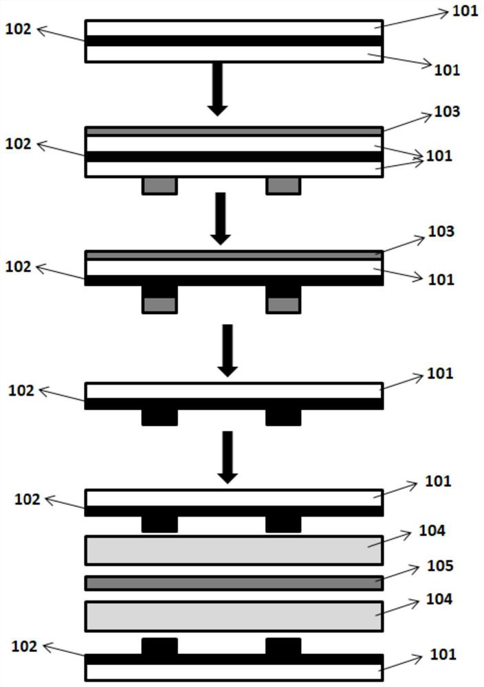
[0036] Step 1) as in figure 2 As shown, prepare two pieces of copper foil 101 with a thickness of 25 μm, and cover the surface of one of the copper foils 101 with acrylic resin 102 with a thickness of 20 μm to obtain a resin copper foil, and quickly press the resin copper foil and the other piece of copper foil 101 together, The rapid pressing conditions are temperature 120° C.; pressure 15 Psi; time 5 min. Then bake and cure, the condition parameters of bake and cure are: temperature 130°C; time 1.5h. get the substrate;
[0037] Step 2) Covering the dry film 103 on one side of the substrate, and pasting the dry film 103 on the other side according to the preset printed pattern, and then etching the substrate covered with the dry film 103 to obtain a sheet with the printed pattern;
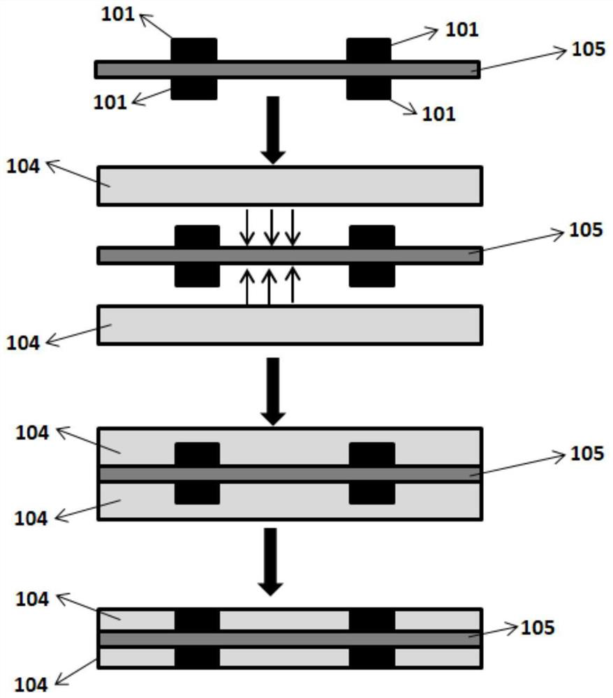
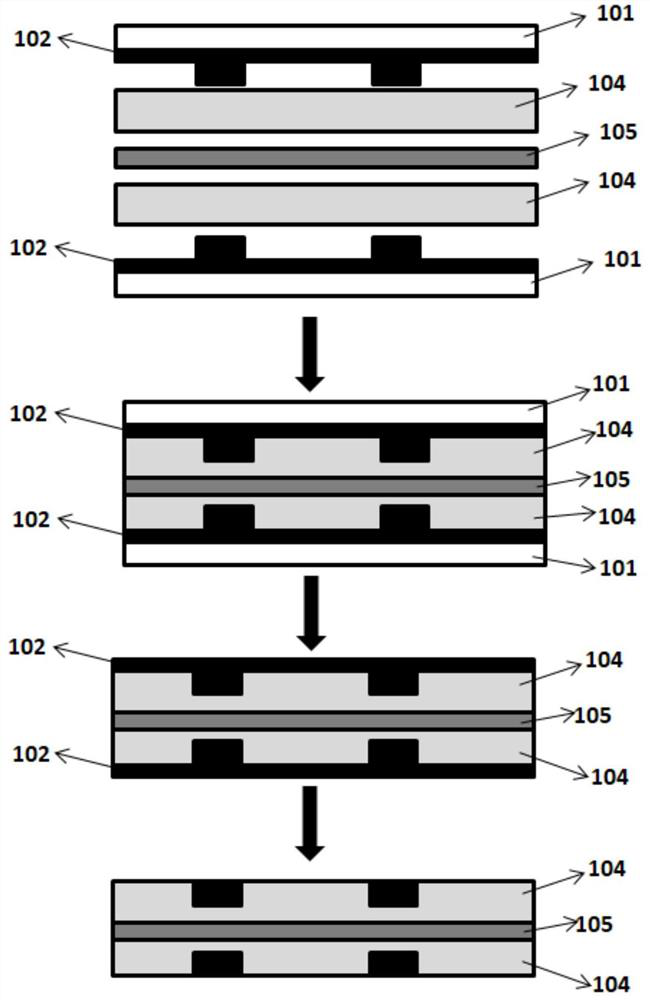
[0038] Step 3) as in image 3 As shown, the sheet, the prepreg 104 and the insulating substrate ...
Embodiment 2
[0041] A method for processing circuit flush printed boards, comprising the following steps:
[0042] Step (1) as figure 2 As shown, one side of the copper foil 101 is covered with a layer of acrylic resin 102 with a total thickness of 15 μm by spraying. It is beneficial to subsequent removal. The thickness of copper foil 101 depends on the design requirements of printed graphics. Generally, the thickness of copper foil 101 should be ≥ 18 μm. In this embodiment, the thickness of copper foil 101 is 18 μm to ensure sufficient Rigidity and maneuverability.
[0043] Step (2) Use the copper foil 101 of the same thickness, and carry out fast pressing with the copper foil 101 coated with acrylic resin 102 under vacuum conditions. The fast pressing conditions are temperature 150° C.; pressure 15 Psi; time 4 minutes. After rapid pressing, bake at 120°C for 2 hours to cure the resin layer.
[0044] Step (3) Cover the fast-pressed material with a dry film 103 on one side for protecti...
Embodiment 3
[0050] A method for processing circuit flush printed boards, comprising the following steps:
[0051] Step (1) Coating a layer of acrylic resin 102 with a total thickness of 5 μm on one side of the copper foil 101 by spraying or rolling, and the thickness of the copper foil 101 is 20 μm.
[0052] Step (2) Use the copper foil 101 of the same thickness, and carry out rapid pressing with the copper foil 101 coated with acrylic resin 102 under vacuum conditions, the rapid pressing conditions are temperature 100° C.; pressure 10 Psi; time 1 min. After rapid pressing, bake at 100°C for 1 hour to cure the resin layer. The purpose of selecting copper foils 101 with the same thickness is to maintain overall symmetry and reduce bending caused by different expansions of materials.
[0053] Step (3) Cover the fast-pressed material with a dry film 103 on one side for protection, and cover the other side with a dry film 103 according to the required printed pattern for protection, and then r...
PUM
| Property | Measurement | Unit |
|---|---|---|
| Thickness | aaaaa | aaaaa |
| Thickness | aaaaa | aaaaa |
| Thickness | aaaaa | aaaaa |
Abstract
Description
Claims
Application Information
 - R&D Engineer
- R&D Manager
- IP Professional
- Industry Leading Data Capabilities
- Powerful AI technology
- Patent DNA Extraction
Browse by: Latest US Patents, China's latest patents, Technical Efficacy Thesaurus, Application Domain, Technology Topic.
© 2024 PatSnap. All rights reserved.Legal|Privacy policy|Modern Slavery Act Transparency Statement|Sitemap