Eureka AIR delivers breakthrough ideas for toughest innovation challenges, trusted by R&D personnel around the world.

Printed circuit board via hole semi-windowing processing device and processing method

A technology for printed circuit boards and processing devices, applied in the directions of printed circuits, manufacturing tools, printed circuit manufacturing, etc., can solve problems such as ink splattering on the pads, affecting the quality of electronic products, and affecting the reliability of printed circuit boards soldering. , to ensure the quality of solder mask, improve adaptability and flexibility, and improve the effect of adaptability

Active Publication Date: 2021-06-25
四川英创力电子科技股份有限公司
View PDF13 Cites 7 Cited by
  • Summary
  • Abstract
  • Description
  • Claims
  • Application Information

AI Technical Summary

Problems solved by technology

According to the current routine process of solder resist processing for half-opened vias, during the exposure process of the solder resist production process of half-opened vias, the part of the vias that is windowed has not received ultraviolet light, and no cross-linking and curing have occurred. Response, during the post-baking process, the ink in the hole is exposed to high temperature and easily overflows the hole to form an oil pad. The oil pad will affect the subsequent soldering reliability of the printed circuit board, thereby affecting the quality of the entire electronic product.

Method used


Image

  • Printed circuit board via hole semi-windowing processing device and processing method
  • Printed circuit board via hole semi-windowing processing device and processing method
  • Printed circuit board via hole semi-windowing processing device and processing method

Examples


Embodiment Construction

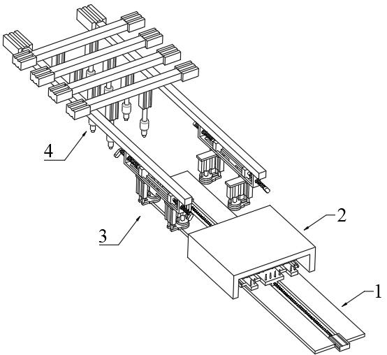
[0046] In order to make the purpose, technical solutions and advantages of the embodiments of the present invention clearer, the embodiments of the present invention will be described in detail below in conjunction with the accompanying drawings, but the embodiments described in the present invention are some of the embodiments of the present invention, not all of them .

[0047] It should be noted that like numerals and letters denote similar items in the following figures, therefore, once an item is defined in one figure, it does not require further definition and explanation in subsequent figures.

[0048] In describing the present invention, it should be noted that the terms "centre", "upper", "lower", "left", "right", "vertical", "horizontal", "inner", "outer" etc. indicate The orientation or positional relationship of the invention is based on the orientation or positional relationship shown in the drawings, or the orientation or positional relationship that is usually p...


PUM


Abstract

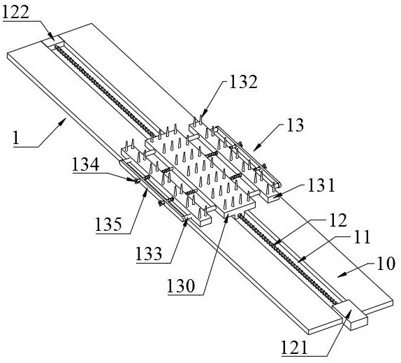
The invention provides a printed circuit board via hole semi-windowing processing device and method. The device comprises a first conveying mechanism, a baking mechanism, a second conveying mechanism, and a board grinding mechanism; the first conveying mechanism comprises a conveying guide rail and a printed circuit board supporting assembly arranged on the conveying guide rail, and the printed circuit board supporting assembly is used for bearing and supporting a printed circuit board to be dried; the second conveying mechanism comprises a pair of longitudinal linear mechanisms arranged in a spaced mode and an adjusting frame connected to linear guide rails of the longitudinal linear mechanisms, and two clamping assemblies are arranged on the adjusting frame; and the board grinding mechanism comprises a transverse linear assembly, a grinding lifting air cylinder, a grinding lifting air cylinder, a grinding motor and a grinding head. Between a hole plugging process of semi-windowing via hole processing and a screen printing plate surface resistance welding process, printed circuit board hole plugging ink is dried in an automatic mode, the situation that after-baking is carried out after development, ink overflows and influences a welding area is avoided, board grinding is automatically carried out on an intersecting windowing area to remove ink, and the resistance welding quality is guaranteed.

Description

technical field [0001] The invention belongs to the field of production and processing of printed circuit boards, and in particular relates to a processing device and method for processing semi-opened through-hole windows of printed circuit boards. Background technique [0002] In printed circuit boards, holes used for conduction or heat dissipation are called vias, and vias are not used for soldering components. In most printed circuit designs, vias are filled and covered with solder mask. The pad is a functional unit used for soldering components on the printed circuit board. During the solder mask process, the solder mask at the position of the pad needs to be windowed. With the improvement of the refinement of electronic products, the wiring design on the printed circuit board is becoming more and more dense, and the solder mask window of the via hole and the pad intersects, resulting in a half-open window of the via hole, such as Figure 10 shown. According to the cur...

Claims


Application Information

Patent Timeline
IPC IPC(8): H05K3/22H05K3/00B24B27/033B24B41/00
CPCB24B27/033B24B41/005H05K3/0094H05K3/227
Inventor 李清华胡志强张仁军牟玉贵杨海军
Owner 四川英创力电子科技股份有限公司
Why Eureka
Eureka Blog
Learn More