
Polarization-independent electro-optical modulator based on two-dimensional grating coupling

An electro-optic modulator and two-dimensional grating technology, applied in the direction of optical waveguide light guide, light guide, optics, etc., can solve the problems of single channel, increase the cost of chip packaging, and cannot realize the modulation of light intensity, etc., achieve high coupling efficiency and improve microwave loss, effect of good impedance matching design

Inactive Publication Date: 2021-06-11
苏州微光电子融合技术研究院有限公司
View PDF4 Cites 3 Cited by
  • Summary
  • Abstract
  • Description
  • Claims
  • Application Information

AI Technical Summary

Problems solved by technology

[0006] 1. This solution technology can only realize the modulation of the light phase, but cannot realize the modulation of the light intensity
[0007] 2. In the prior art, the optical fiber and the grating coupler are obliquely coupled. The angle of the optical fiber needs to be tuned during on-chip testing, and angle polishing is required when the optical fiber is packaged, which virtually increases the packaging cost of the chip.
[0008] 3. In the prior art, only two-channel transmission can be realized, and the channel is relatively single

Method used


Image

  • Polarization-independent electro-optical modulator based on two-dimensional grating coupling
  • Polarization-independent electro-optical modulator based on two-dimensional grating coupling
  • Polarization-independent electro-optical modulator based on two-dimensional grating coupling

Examples


Embodiment Construction

[0030] The present invention will be described in detail below in conjunction with various embodiments shown in the drawings. However, these embodiments do not limit the present invention, and structural, method, or functional changes made by those skilled in the art according to these embodiments are included in the protection scope of the present invention.

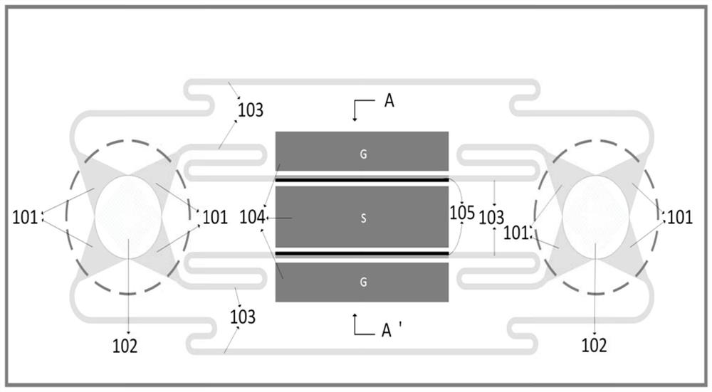
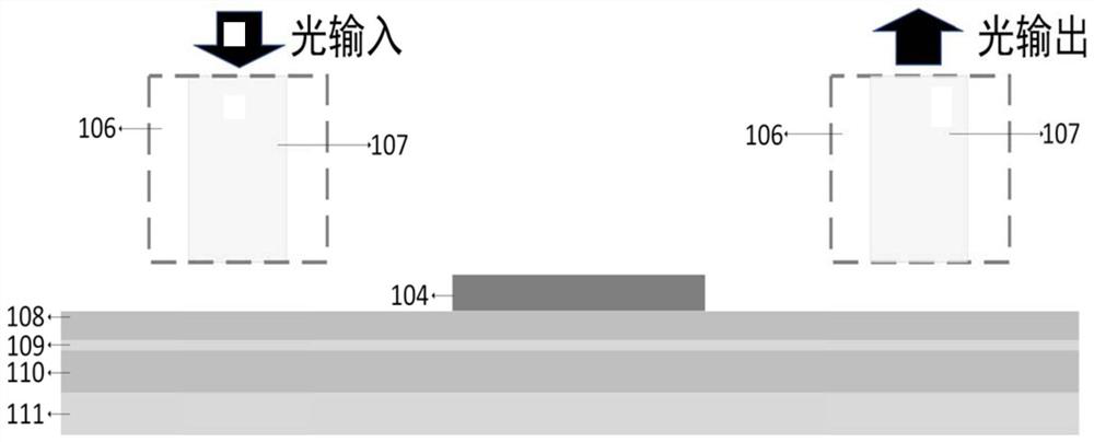
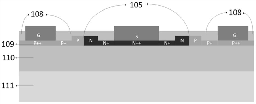
[0031] This embodiment provides a polarization-independent electro-optic modulator based on two-dimensional grating coupling, such as Figure 1-4 , including substrate 111, lower cladding layer 110, silicon device layer 109, upper cladding layer 108 from bottom to top, and eight mode spot converters 101 and four silicon substrates formed by etching on silicon device layer 109 Optical waveguide 103, two four-channel input\output two-dimensional grating couplers 102, two silicon-based PN junction optical waveguide phase shifters 105, and a GSG single-drive coplanar waveguide traveling wave electrode 104.

[0032] Among t...


PUM

PropertyMeasurementUnit
thicknessaaaaaaaaaa

Abstract

The invention provides a polarization-independent electro-optical modulator based on two-dimensional grating coupling. The polarization-independent electro-optical modulator sequentially comprises: a substrate, a lower cladding, a silicon device layer and an upper cladding from bottom to top, eight spot size converters, four silicon-based optical waveguides, two four-channel input\output two-dimensional grating couplers, two silicon-based PN junction optical waveguide phase shifters and a GSG single-drive coplanar waveguide traveling wave electrode which are formed on the silicon device layer in an etching mode, wherein the silicon-based PN junction optical waveguide phase shifters are of waveguide structures made of silicon materials. The middle section of the at least two silicon-based optical waveguides is replaced by a waveguide structure, and the GSG single-drive coplanar waveguide traveling wave electrode is arranged above the silicon-based PN junction optical waveguide phase shifter and is in contact with a flat plate area of the silicon-based PN junction optical waveguide phase shifter. Light beam splitting and light beam combination of four channels can be achieved, conversion from light phase modulation to light intensity modulation can be achieved, in addition, the optical fiber and the grating coupler are vertically coupled, and the advantages of being high in coupling efficiency, low in polarization dependent loss and high in alignment tolerance capacity are achieved.

Description

technical field [0001] The invention belongs to silicon-based photonics and chip-level optical interconnection technology, in particular to a polarization-independent electro-optical modulator based on two-dimensional grating coupling. Background technique [0002] In the modern society with the rapid development of science and technology, a large amount of information and data exchange requires a high-speed, broadband communication system. With the continuous decline of integrated circuit process nodes, the limitations of microelectronics processes are becoming more and more obvious. On the one hand, due to the continuous reduction of device line width, the traditional photolithography processing method is close to the limit; on the other hand, due to the synchronous reduction of transistor size and interconnection line size, the delay and power consumption of a single transistor are getting worse and worse. Smaller, while the delay and power consumption of the interconnec...

Claims


Application Information

Patent Timeline
Patent Type & Authority Applications(China)
IPC IPC(8): G02F1/01G02F1/025G02B6/12
CPCG02F1/011G02F1/025G02B6/12G02B2006/12038G02B2006/12097
Inventor 黄北举张赞允
Owner 苏州微光电子融合技术研究院有限公司
Learn More