MEMS inertial sensor low-stress packaging structure and method based on graphical gold-tin soldering

An inertial sensor and packaging method technology, applied in the field of micro-electromechanical, can solve problems affecting device reliability, reduce packaging stress, reduce vibration and shock resistance, etc., to reduce effective contact area, reduce packaging stress, and structural rigidity big effect

Active Publication Date: 2021-06-11
NANJING UNIV OF SCI & TECH
View PDF8 Cites 0 Cited by
  • Summary
  • Abstract
  • Description
  • Claims
  • Application Information

AI Technical Summary

Problems solved by technology

The MEMS inertial sensor patch process often uses adhesives, such as epoxy resin, silver glass, etc. The use of low-hardness adhesives can effectively reduce the packaging stress. However, due to the strong temperature characteristics of the adhesive material, high and low temperature When the Young's modulus changes nonlinearly, the output of the MEMS inertial sensor has a high-order relationship with the temperature, which is difficult to compensate; in addition, the adhesive will produce outgassing, etc., which is not suitable for MEMS inertial sensors packaged in device-level vacuum
The size of the bonding area of ​​the MEM inertial sensor chip will also affect the packaging stress. Therefore, a low-stress packaging solution (CN103193198A) with adhesive graphics is proposed. The smaller the bonding area, the smaller the stress. At the same time, the bonding strength of the chip smaller, which affects the reliability of the device
The idea of ​​stress isolation is to add a transition structure (CN109761187A) between the MEMS inertial sensor chip and the shell. The smaller the stiffness of the transition structure, the better the isolation effect. However, when the transition structure is small, it cannot improve the stability of the MEMS inertial sensor. The benchmark, causing measurement errors, the second is to reduce the vibration and shock resistance

Method used


Image

  • MEMS inertial sensor low-stress packaging structure and method based on graphical gold-tin soldering
  • MEMS inertial sensor low-stress packaging structure and method based on graphical gold-tin soldering
  • MEMS inertial sensor low-stress packaging structure and method based on graphical gold-tin soldering

Examples


Embodiment Construction

[0015] The present invention will be further introduced below in conjunction with the accompanying drawings and specific embodiments.

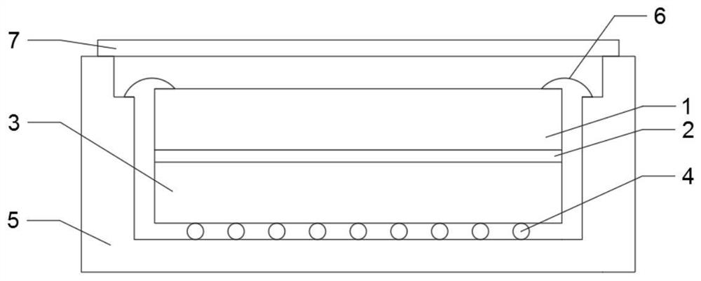
[0016] The present invention is based on the MEMS inertial sensor low-stress packaging structure of patterned gold-tin soldering, including MEMS inertial sensor chip 1, adhesive glue 2, transition layer 3, gold-tin soldering layer 4, packaging tube shell 5, lead wire 6 and cover plate 7 .

[0017] to combine figure 1 The material of the package shell 5 is ceramic or metal, the shape is rectangular or circular, and the bottom of the cavity of the package shell 5 is plated with a layer of gold.

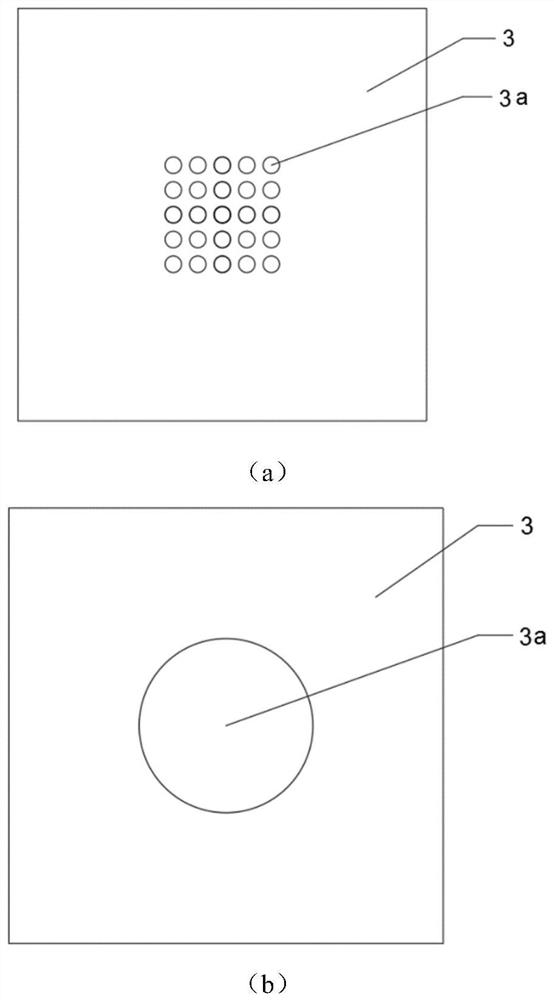
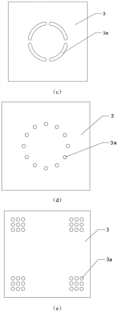
[0018] The material of the transition layer 3 is the same as the substrate material of the MEMS inertial sensor chip, which is silicon or glass. A patterned gold layer 3a is plated on the bottom of the transition layer 3 using a MEMS process.

[0019] The transition layer 3 is welded on the package shell 5 by gold-tin soldering process, and a pattern...


PUM


Abstract

The invention discloses an MEMS inertial sensor low-stress packaging structure and method based on graphical gold-tin soldering. An MEMS inertial device comprises an MEMS sensor chip, bonding glue, a transition layer, gold-tin soldering and a packaging tube shell. The MEMS sensor chip is bonded on the transition layer through the bonding glue, and the transition layer is welded on the packaging tube shell through gold tin soldering. The transition layer is additionally arranged between the MEMS sensor chip and the packaging tube shell, so that stress generated by deformation of the ceramic tube shell is concentrated at the bottom of the transition layer; and through gold-tin soldering patterning, important anchor points of the MEMS sensor chip are avoided, the contact area between the transition layer and the packaging tube shell is reduced, the influence of packaging stress on the sensitive structure of the MEMS inertial device is finally reduced, and the purpose of improving the precision of the MEMS inertial device is achieved.

Description

technical field [0001] The invention relates to the field of micro-electromechanical technology, in particular to a MEMS inertial sensor low-stress packaging structure and method based on patterned gold-tin soldering. Background technique [0002] MEMS packaging is a process that MEMS sensors must go through before the chip is formed. It supports and protects the chip from interference and damage from the external environment. In addition, for different MEMS sensors, their packaging also needs to provide a corresponding working environment and activity space. [0003] The residual stress in MEMS sensors mainly comes from the MEMS chip preparation process and packaging process. After the chip undergoes processes such as oxidation and etching during the manufacturing process, residual stress will appear in the microstructure, which is called process stress. The process stress is determined by the process. Since the silicon crystal structure is stable, it has little impact on...

Claims


Application Information

Patent Timeline
Patent Type & Authority Applications(China)
IPC IPC(8): B81B7/00B81B7/02B81C1/00
CPCB81B7/0045B81B7/02B81C1/00325B81B2201/0228Y02P70/50
Inventor 施芹裘安萍夏国明赵阳贡旭超
Owner NANJING UNIV OF SCI & TECH
Why Eureka
Try Eureka