Optical hypersurface material, application and macromolecular substance transepidermal cell introduction method
A technology of macromolecular substances and epidermal cells, which is applied in the field of macromolecular substances trans-epidermal cell import and optical metasurface materials, which can solve the problems of limited penetration into the dermis, low efficiency, and long treatment cycle.
- Summary
- Abstract
- Description
- Claims
- Application Information
AI Technical Summary
Problems solved by technology
Method used
Image
Examples
preparation example Construction
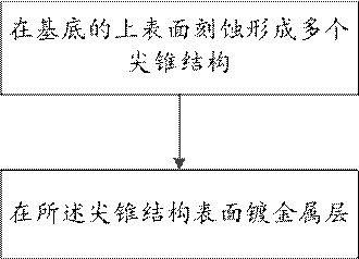
[0037] The present invention also proposes a preparation method of an optical metasurface material, please refer to figure 2 ,include:
[0038] A plurality of pointed cone structures are formed by etching on the upper surface of the substrate.
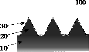
[0039] Specifically, the substrate may be, for example, a silicon wafer, or titanium dioxide or silicon dioxide. The base includes an upper surface and a lower surface oppositely disposed.
[0040] Specifically, a plurality of pointed cone structures are formed by etching on the upper surface of the substrate. The pointed cone structures may be, for example, pyramid-shaped, but not limited thereto, and may also be triangular-conical, conical, or other irregular conical shapes. etc., it is enough to make the pointed cone structure have a point.
[0041] Specifically, the size of the pointed cone structure is on the order of submicron to micron, and is adjusted with reference to the size of the acting cells.
[0042] More specifical...
Embodiment 1
[0076] The preparation process of the optical metasurface material of embodiment 1 is as follows:
[0077] 1. Wet etching forms a pyramid-shaped cone structure on the surface of the silicon wafer
[0078] 1. Using plasma enhanced chemical vapor deposition (PECVD) to deposit a layer of silicon nitride (Si 3 N 4 ) film, after coating, spin coat a layer of photoresist and cover the mask plate, use a photolithography machine for exposure treatment, and obtain a circular Si after development and etching 3 N 4 mask layer;
[0079]2. Then use acetone and deionized water to ultrasonically clean the silicon wafer to remove residual photoresist and ensure the cleanliness of the silicon wafer;
[0080] 3. Finally, carry out alkali etching on the silicon wafer, use the mixed solution of potassium hydroxide, water and isopropanol as the alkali etching solution, and carry out alkali etching on the silicon wafer. Based on the principle of anisotropic etching, by controlling the etching ...
Embodiment 2
[0084] The difference between the optical metasurface material of Example 2 and Example 1 is that the metal plated on the surface of the conical structure is not gold, but silver-plated, and the other steps are the same as in Example 1, and will not be repeated here.
PUM
| Property | Measurement | Unit |
|---|---|---|
| wavelength | aaaaa | aaaaa |
| diameter | aaaaa | aaaaa |
| diameter | aaaaa | aaaaa |
Abstract
Description
Claims
Application Information
 - R&D
- Intellectual Property
- Life Sciences
- Materials
- Tech Scout
- Unparalleled Data Quality
- Higher Quality Content
- 60% Fewer Hallucinations
Browse by: Latest US Patents, China's latest patents, Technical Efficacy Thesaurus, Application Domain, Technology Topic, Popular Technical Reports.
© 2025 PatSnap. All rights reserved.Legal|Privacy policy|Modern Slavery Act Transparency Statement|Sitemap|About US| Contact US: help@patsnap.com


