LIGBT device with integrated NMOS transistor
A device and collector technology, applied in the field of LIGBT devices, can solve the problems of increasing device on-voltage drop and reducing anode P+ injection efficiency.
- Summary
- Abstract
- Description
- Claims
- Application Information
AI Technical Summary
Problems solved by technology
Method used
Image
Examples
Embodiment 1
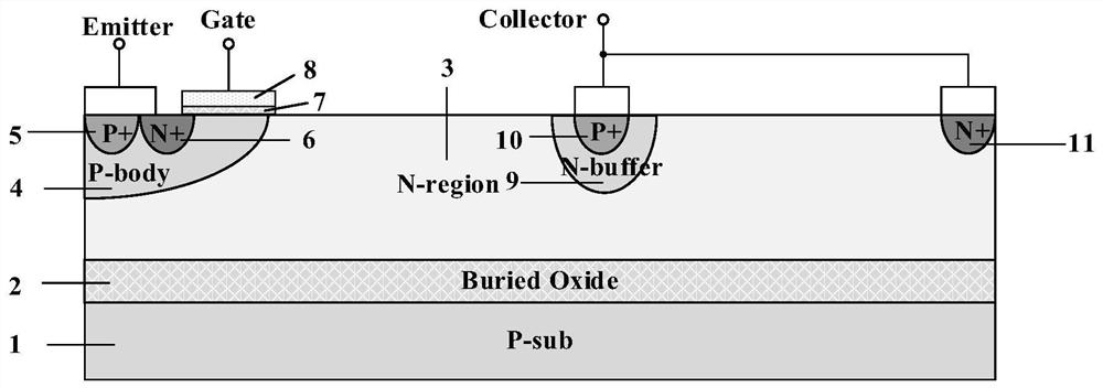
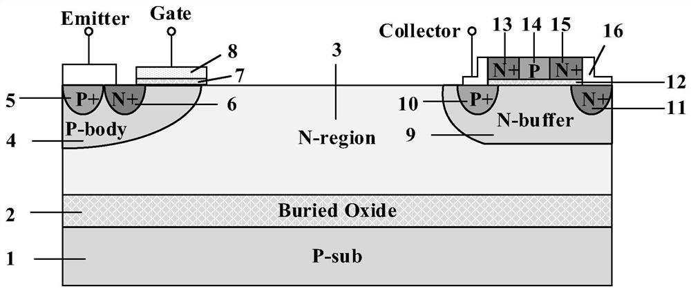
[0020] Such as image 3 As shown, this example includes a bottom-up P substrate 1, an insulating dielectric buried layer 2, and a top semiconductor layer; the top semiconductor layer includes an emitter structure, a gate structure, an N drift region 3, and a collector structure; The emitter structure includes a P well region 4, a P+ body contact region 5 and an N+ emitter region 6, the P+ body contact region 5 and the N+ emitter region 6 are located on the upper surface of the P well region 4, and the N+ emitter region 6 is located near the N drift On one side of the region 3, the emitter is jointly drawn from the surface of the P+ body contact region 5 and the N+ emitter region 6; the gate structure includes a gate oxide layer 7 and a gate polysilicon 8 covering the gate oxide layer 7, and the gate oxide layer 7 Located on the P well region 4 and the two ends overlap with the N+ emitter region 6 and the N drift region 3 respectively, and the lead-out end of the gate polysilic...
Embodiment 2
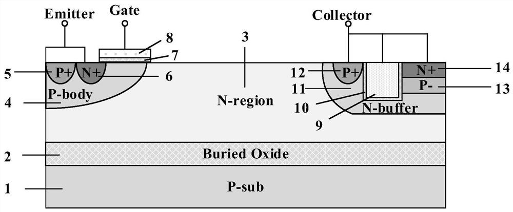
[0024] Such as Figure 4 As shown, compared with Embodiment 1, the N+ collector region 11 is located on the surface of the N drift region 3 in this example. The N+ collector region 11 is located on the surface of the N drift region 3, which can effectively alleviate the pressure of the integrated NMOS region to suppress the Snapback effect, so that the snapback effect can be effectively suppressed at a lower concentration of the P-channel region, and the electrons stored in the drift region can be further accelerated. The extraction reduces the turn-off time and turn-off loss.
Embodiment 3
[0026] Such as Figure 5 As shown, compared with Embodiment 1, the P+ collector electrode 10 overlaps with the N+ source region 13 and the P-type channel region 14 in this example. The P+ collector 10 has no depletion effect on the P-channel region 14 above it, so the snapback phenomenon can be suppressed at a lower doping concentration of the P-channel region, and the extraction of electrons stored in the drift region can be further accelerated , reducing the turn-off time and turn-off loss.
PUM
 Abstract
Description
Claims
Application Information
 - R&D
- Intellectual Property
- Life Sciences
- Materials
- Tech Scout
- Unparalleled Data Quality
- Higher Quality Content
- 60% Fewer Hallucinations
Browse by: Latest US Patents, China's latest patents, Technical Efficacy Thesaurus, Application Domain, Technology Topic, Popular Technical Reports.
© 2025 PatSnap. All rights reserved.Legal|Privacy policy|Modern Slavery Act Transparency Statement|Sitemap|About US| Contact US: help@patsnap.com


