Preparation method of source and drain electrodes of high-electron-mobility transistor
A high electron mobility, source-drain electrode technology, applied in the direction of circuits, electrical components, semiconductor devices, etc., to reduce costs, reduce error requirements, and improve performance
- Summary
- Abstract
- Description
- Claims
- Application Information
AI Technical Summary
Problems solved by technology
Method used
Image
Examples
Embodiment 1
[0046] Example 1: Preparation of InP-based high electron mobility transistor source and drain electrodes by corner evaporation self-alignment process
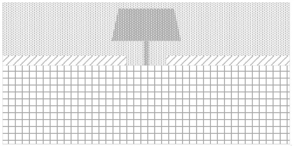
[0047] (1) Select a T-shaped gate with a gate width of 30nm, a gate height of 150nm, a gate width of 500nm, a height of 200nm, and an InP-based high electron mobility transistor substrate with a gate groove corrosion depth of 20nm. Such as Figure 8 shown;
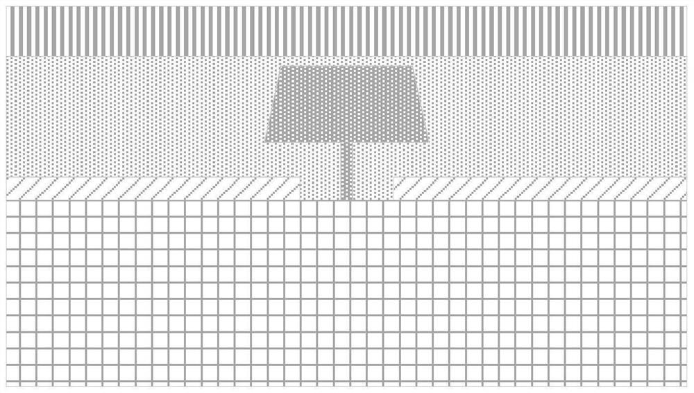
[0048](2) Spin-coat the LOR sacrificial layer on the substrate at a speed of 4000 RPM, and bake it in an oven at 180°C for 30 minutes to cure and take it out, such as Figure 9 shown;
[0049] (3) Continue to spin-coat AZ5214 photoresist on the substrate at a speed of 4000RPM, and bake it on a hot plate at 95°C for 90 seconds to cure. The result is as follows: Figure 10 shown;
[0050] (4) The sample is subjected to an overlay exposure treatment of 6.25mW / cm in a contact optical lithography machine 2 The power exposure is 6.7s. The result is as Figure 11 shown;
...
PUM
| Property | Measurement | Unit |
|---|---|---|
| height | aaaaa | aaaaa |
| width | aaaaa | aaaaa |
| depth | aaaaa | aaaaa |
Abstract
Description
Claims
Application Information
 - R&D
- Intellectual Property
- Life Sciences
- Materials
- Tech Scout
- Unparalleled Data Quality
- Higher Quality Content
- 60% Fewer Hallucinations
Browse by: Latest US Patents, China's latest patents, Technical Efficacy Thesaurus, Application Domain, Technology Topic, Popular Technical Reports.
© 2025 PatSnap. All rights reserved.Legal|Privacy policy|Modern Slavery Act Transparency Statement|Sitemap|About US| Contact US: help@patsnap.com


