
Preparation method of transmission electron microscope sample

A technique for TEM samples and samples, which is applied in the preparation, sampling, and sampling devices of test samples, and can solve the problems of inconsistent cutting speed, curtain effect, and easy to produce stretch marks.

Pending Publication Date: 2022-05-13
GIGA FORCE ELECTRONICS CO LTD
View PDF0 Cites 0 Cited by
  • Summary
  • Abstract
  • Description
  • Claims
  • Application Information

AI Technical Summary

Problems solved by technology

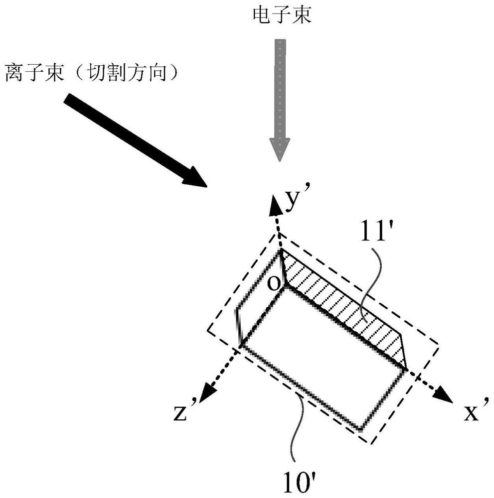
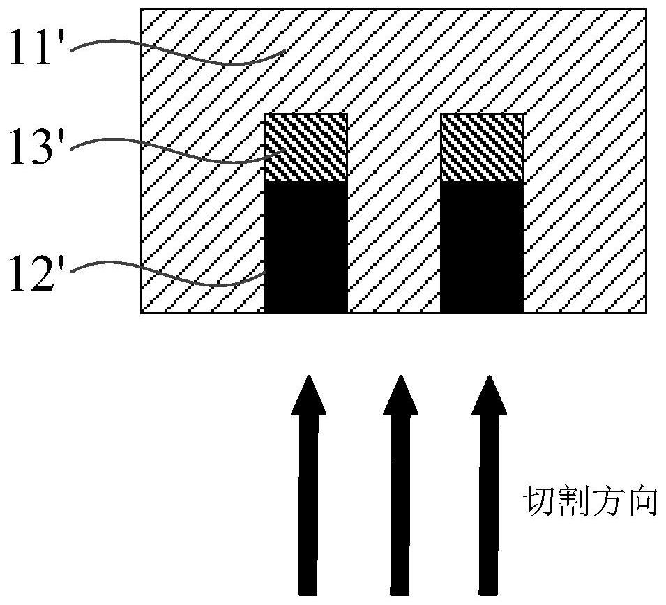
[0003] In the existing cutting method, due to the different components on the surface of the sample to be prepared, the cutting speed for different components is inconsistent, and the cutting effect is also different. If the more difficult to cut components come first, the easier to cut components will follow. It is easy to produce pull marks, that is, to produce curtain effect

Method used


Image

  • Preparation method of transmission electron microscope sample
  • Preparation method of transmission electron microscope sample
  • Preparation method of transmission electron microscope sample

Examples


preparation example Construction

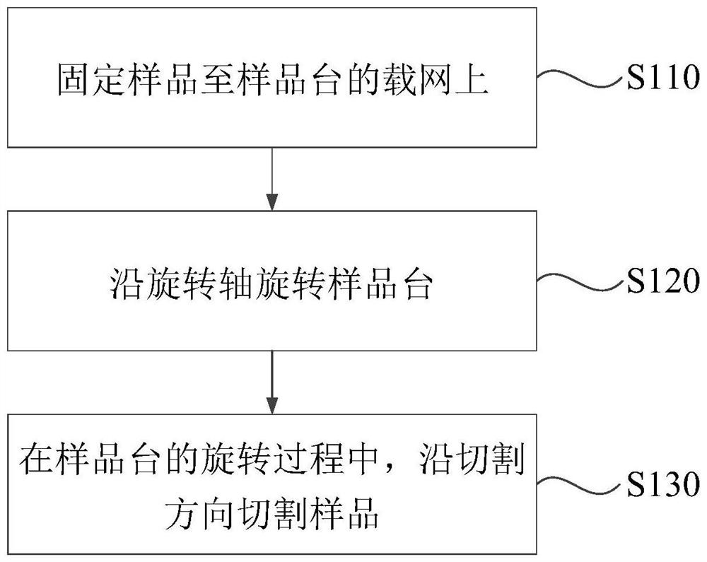
[0044] figure 1 A flow chart of a method for preparing a transmission electron microscope sample provided by an embodiment of the present invention, such as figure 1 Shown, this preparation method comprises:

[0045] S110, fixing the sample on the carrier grid of the sample stage.

[0046] Specifically, firstly, the carrier net can be installed on the sample platform, and then the sample can be fixed on the carrier net. Carrier grid is a common vocabulary in the field of transmission electron microscope sample preparation, and it can also be called copper grid, microgrid, etc. The type of carrier grid can be selected according to actual needs, which is not limited in the embodiment of the present invention. It can be understood that the above-mentioned sample is a tiny sample including the position to be detected, and the sample includes a surface to be thinned, and in the subsequent sample preparation process, the surface to be thinned of the sample is cut to thin the sampl...


PUM


Abstract

The invention discloses a preparation method of a transmission electron microscope sample. The method comprises the following steps: fixing the sample to a carrying net of a sample table; rotating the sample table along a rotating shaft, wherein the extending direction of the rotating shaft is parallel to the normal direction of the to-be-thinned surface of the sample; in the rotating process of the sample table, the sample is cut in the cutting direction, and the cutting direction is parallel to the plane where the surface to be thinned is located. According to the technical scheme, in the sample cutting process, the cutting direction is always parallel to the plane where the to-be-thinned surface is located, by changing the rotating angle of the sample table, the cutting light beam can directly cut part of the area behind the component difficult to cut at a certain angle, drawing marks are reduced, and the cutting efficiency is improved. The cutting thickness of the surface to be thinned is more uniform, the thickness of the prepared transmission electron microscope sample is more uniform, and the success rate of sample preparation is improved; and the thickness of the prepared transmission electron microscope sample is relatively uniform, so that convenience can be provided for subsequent observation and analysis.

Description

technical field [0001] The invention relates to the field of semiconductor manufacturing and analysis, in particular to a method for preparing a transmission electron microscope sample. Background technique [0002] At present, with the rapid development of semiconductor technology, the demand for chip research and development and failure analysis is increasing day by day. For small process chips or chips with small failure points, the sample is usually cut to thin the sample to a smaller thickness, that is, the sample A tiny structure that can be observed with a transmission electron microscope (Transmission Electron Microscope, TEM) is made, so as to analyze the point of failure of the sample. [0003] In the existing cutting method, due to the different components on the surface of the sample to be prepared, the cutting speed for different components is inconsistent, and the cutting effect is also different. If the more difficult to cut components come first, the easier t...

Claims


Application Information

Patent Timeline
Patent Type & Authority Applications(China)
IPC IPC(8): G01N1/06G01N1/28
CPCG01N1/06G01N1/28G01N1/286G01N2001/2873
Inventor 高强郑朝晖
Owner GIGA FORCE ELECTRONICS CO LTD
Learn More