
LDMOS device manufacturing method, LDMOS device and terminal equipment

A manufacturing method and device technology, which can be used in semiconductor/solid-state device manufacturing, semiconductor devices, electrical components, etc., and can solve problems such as inability to generate an electron accumulation layer.

Pending Publication Date: 2021-04-09
HUA HONG SEMICON WUXI LTD
View PDF4 Cites 1 Cited by
  • Summary
  • Abstract
  • Description
  • Claims
  • Application Information

AI Technical Summary

Problems solved by technology

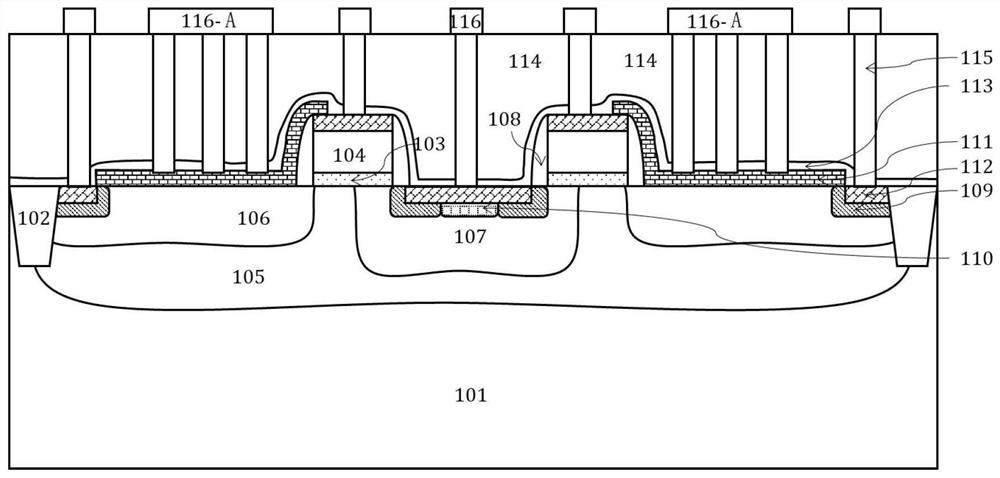
[0003] Existing LDMOS structures such as figure 1 As shown, the field plate for adjusting the electric field is formed by introducing a conductive contact hole on the dielectric layer SAB, but in the traditional structure, 116-A is either directly shorted to the gate or directly shorted to the source
In the on state, the contact hole is shorted to the gate to form an additional electron accumulation layer above the drift region to reduce Rsp, but the gate-drain capacitance is large, and the contact hole is shorted to the source to shield the gate. Reduce gate-drain capacitance, but cannot create an electron accumulation layer, thus increasing Rsp

Method used


Image

  • LDMOS device manufacturing method, LDMOS device and terminal equipment
  • LDMOS device manufacturing method, LDMOS device and terminal equipment
  • LDMOS device manufacturing method, LDMOS device and terminal equipment

Examples


no. 1 example ;

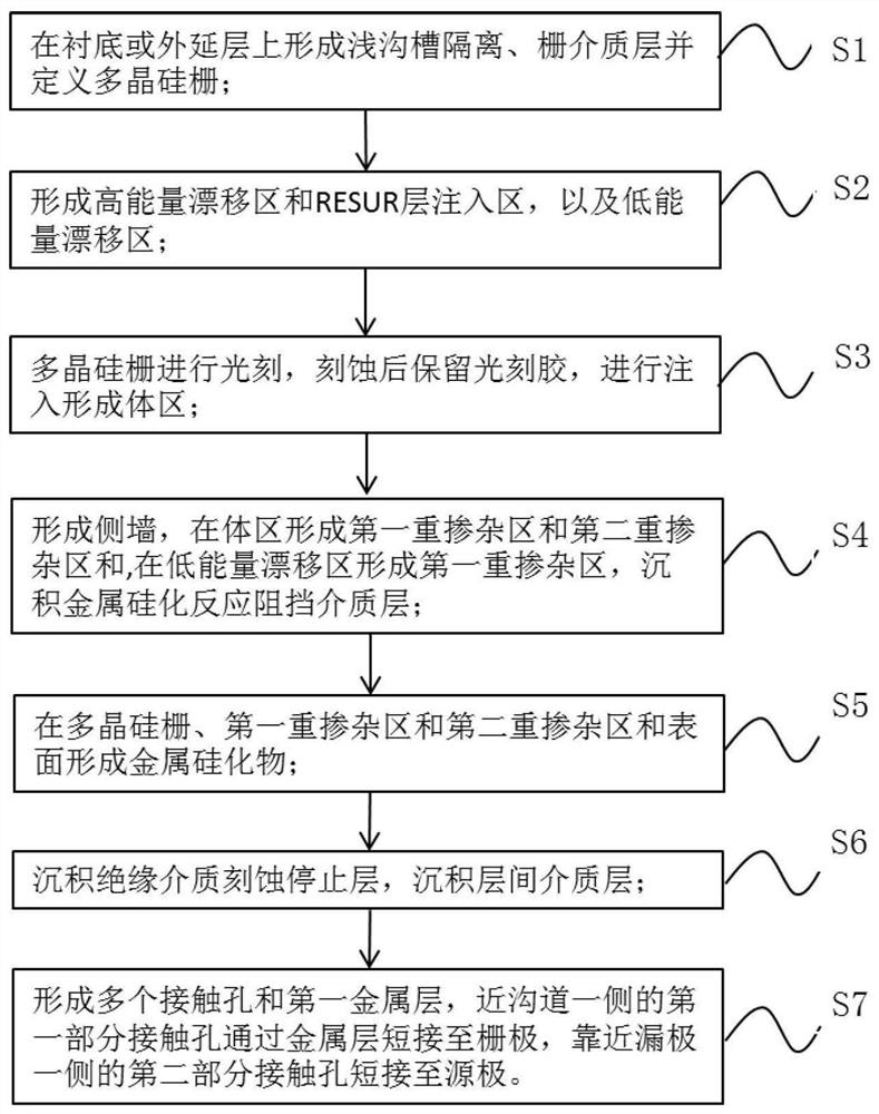
[0048] Such as figure 2 As shown, the present invention provides a kind of LDMOS device manufacturing method, comprises the following steps:

[0049] S1, forming shallow trench isolation 102 on the substrate or epitaxial layer 101, then forming a gate dielectric layer 103, depositing and forming a polysilicon layer, and etching to define a polysilicon gate 104 at the same time;

[0050] S2, coating the photoresist 501 and opening the photoresist in the LDMOS region, performing drift region and RESURF implantation, forming a high-energy drift region with uneven ion concentration distribution in the lateral direction, a RESUR layer implantation region 105, and a low-energy drift region 106 ;

[0051] S3, performing photolithography on the defined polysilicon gate 104, retaining the photoresist after etching, and performing implantation to form the body region 107;

[0052] S4, form sidewalls 108 on both sides of the polysilicon gate 104, perform highly doped implantation in t...

no. 2 example ;

[0057] The invention provides a method for manufacturing an N-LDMOS device, comprising the following steps:

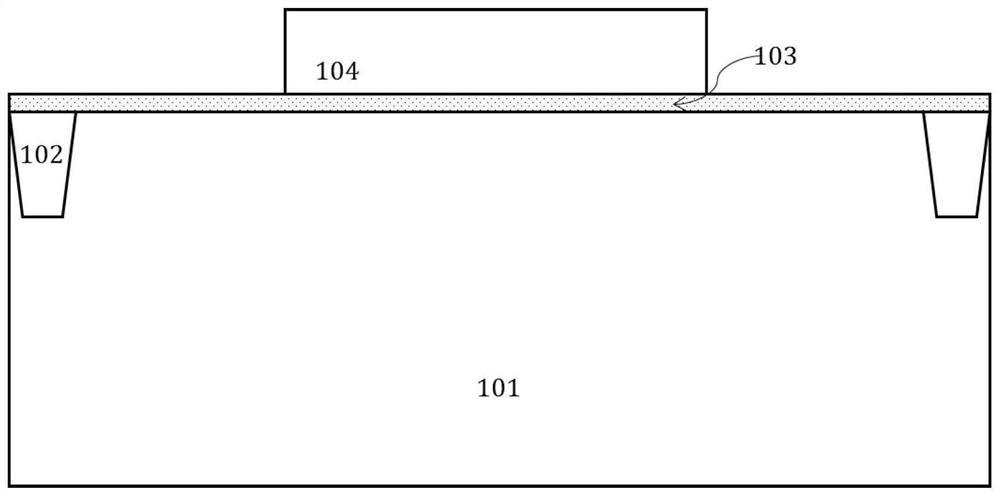
[0058] S1, such as image 3 As shown, shallow trench isolation 102 is formed on 101—P-type substrate / P-type epitaxial layer 101, then thermally oxidized to form a gate dielectric layer 103, deposited to form a polysilicon layer, and etched to define a polysilicon gate 104 at the same time;

[0059] S2, such as Figure 4 As shown, the photoresist 501 is coated and the photoresist in the LDMOS region is opened, and the drift region and RESURFP type implantation are performed to form a high-energy drift region and a RESUR layer implantation region 105 with uneven ion concentration distribution in the lateral direction, and a low-energy drift region. District 106;

[0060] Due to the existence of the defined polysilicon gate 104, high-energy (>80KeV) drift region and RESURF (>300KeV) implants directly pass through the polysilicon gate 104 and enter Silicon, while low-ene...

no. 3 example ;

[0067] Such as Figure 7 As shown, the present invention provides an LDMOS device manufactured by the method for manufacturing an LDMOS device described in any one of the first embodiment or the second embodiment above, including:

[0068] Shallow trench isolation 102 formed in the substrate or epitaxial layer 101;

[0069] High-energy drift region and RESUR layer implant region 105 formed on the substrate or epitaxial layer 101 between shallow trench isolations 102;

[0070] Low energy drift region 106, which is formed on the upper part of substrate or epitaxial layer 101 between shallow trench isolation 102 and body region 107, and adjacent to shallow trench isolation 102;

[0071] a body region 107 formed on top of the substrate or epitaxial layer 101 between the low energy drift regions 106;

[0072] The first heavily doped region 109 is formed on the upper part of the low-energy drift region 106 and the upper part of the body region 107;

[0073] a second heavily doped...


PUM


Abstract

The invention discloses an LDMOS device manufacturing method. The method comprises the following steps: forming shallow trench isolation and a gate dielectric layer on a substrate or an epitaxial layer, and defining a polysilicon gate; forming a high-energy drift region, an RESUR layer injection region and a low-energy drift region; photoetching the polysilicon gate, reserving photoresist after etching, and performing injection to form a body region; forming a side wall, forming a first heavily doped region and a second heavily doped region in the body region, forming a first heavily doped region in the low-energy drift region, and depositing a metal silicification reaction barrier dielectric layer; forming metal silicide on the surfaces of the polysilicon gate, the first heavily doped region and the second heavily doped region; depositing an insulating medium etching stop layer, and depositing an interlayer dielectric layer; and forming a plurality of contact holes and a first metal layer, short-circuiting a first part of contact holes close to one side of a channel to the grid electrode through the metal layer, and short-circuiting a second part of contact holes close to one side of a drain electrode to a source electrode. The invention further discloses an LDMOS device and terminal equipment used for manufacturing the LDMOS device.

Description

technical field [0001] The invention relates to the field of semiconductor manufacturing, in particular to a method for manufacturing an LDMOS device, an LDMOS device and a terminal device for manufacturing the LDMOS device. Background technique [0002] DMOS (Double-diffused MOS) is currently widely used in power management circuits due to its characteristics of high voltage resistance, high current drive capability and extremely low power consumption. In LDMOS (Lateral Double-diffused MOS) devices, on-resistance Rsp and gate-drain capacitance Cgd are two important indicators of LDMOS devices. How to obtain higher breakdown voltage, lower Rsp, and lower Cgd can improve the competitiveness of products. [0003] Existing LDMOS structures such as figure 1 As shown, the field plate for adjusting the electric field is formed by introducing conductive contact holes on the dielectric layer SAB, but in the traditional structure, 116-A is either directly shorted to the gate or dir...

Claims


Application Information

Patent Timeline
IPC IPC(8): H01L21/336H01L29/78H01L29/06
CPCH01L29/66681H01L29/7816H01L29/063
Inventor 许昭昭
Owner HUA HONG SEMICON WUXI LTD
Learn More