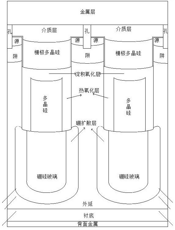
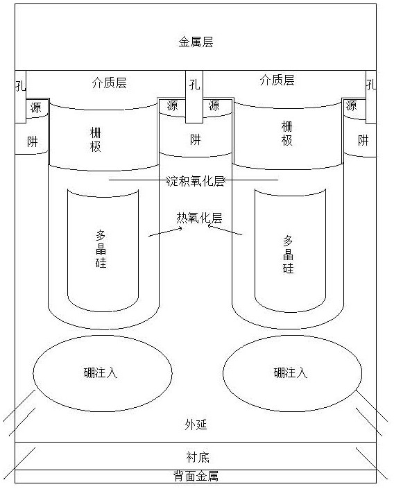
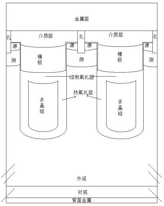
Three-section type oxide layer shielding gate trench MOSFET structure
A technology of oxide layer and shielding grid, applied in the direction of electrical components, circuits, semiconductor devices, etc., can solve problems that hinder the development of advanced SGT
- Summary
- Abstract
- Description
- Claims
- Application Information
AI Technical Summary
Problems solved by technology
Method used
Image
Examples
Embodiment Construction
[0023] The present invention will be described in detail below in combination with specific embodiments.
[0024] The invention relates to a three-stage oxide layer shielded gate trench MOSFET structure. The MOSFET structure is located on an epitaxial substrate, and there is an area under the source trench, which is filled with a material inverse to the epitaxial line and thereby P-column and epitaxy formed by diffusion source diffusion to achieve charge balance.
[0025] The region under the source trench of the MOSFET structure is a deep trench. The filling material area in the deep trench is narrow in width and high in height, the width is in the range of 0.2-2 microns, the height is in the range of 0.5-17 microns, and the depth below the Si surface is between 2 microns and 17 microns. The depth of the deep trench is less than the thickness of the epitaxy on which the MOSFET structure is located.
[0026] The surfaces on both sides of the filling material region in the de...
PUM
 Abstract
Description
Claims
Application Information
 - R&D Engineer
- R&D Manager
- IP Professional
- Industry Leading Data Capabilities
- Powerful AI technology
- Patent DNA Extraction
Browse by: Latest US Patents, China's latest patents, Technical Efficacy Thesaurus, Application Domain, Technology Topic, Popular Technical Reports.
© 2024 PatSnap. All rights reserved.Legal|Privacy policy|Modern Slavery Act Transparency Statement|Sitemap|About US| Contact US: help@patsnap.com


