
Manufacturing method of three-section type oxide layer shielding gate trench MOSFET structure

A manufacturing method and oxide layer technology, applied in semiconductor/solid-state device manufacturing, electrical components, circuits, etc., can solve problems hindering the development of advanced SGT, achieve good high-temperature reflow characteristics, good trench filling ability, and reduce device Rsp Effect

Inactive Publication Date: 2020-11-13
XIAN LONTEN RENEWABLE ENERGY TECH
View PDF4 Cites 6 Cited by
  • Summary
  • Abstract
  • Description
  • Claims
  • Application Information

AI Technical Summary

Problems solved by technology

Single or multiple unequal energy injections cannot achieve a more ideal junction shape, hindering the further development of advanced SGTs

Method used


Image

  • Manufacturing method of three-section type oxide layer shielding gate trench MOSFET structure
  • Manufacturing method of three-section type oxide layer shielding gate trench MOSFET structure
  • Manufacturing method of three-section type oxide layer shielding gate trench MOSFET structure

Examples


Embodiment Construction

[0049] The present invention will be described in detail below in combination with specific embodiments.

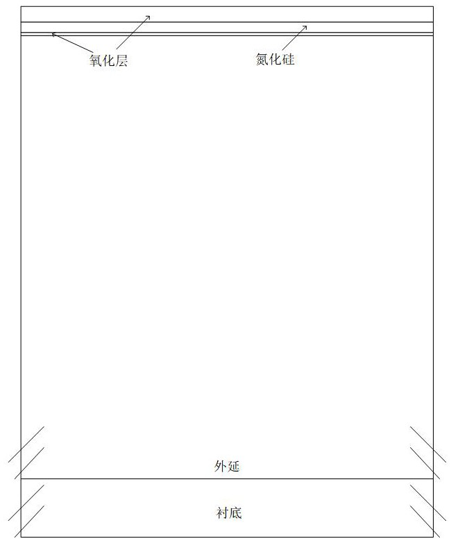
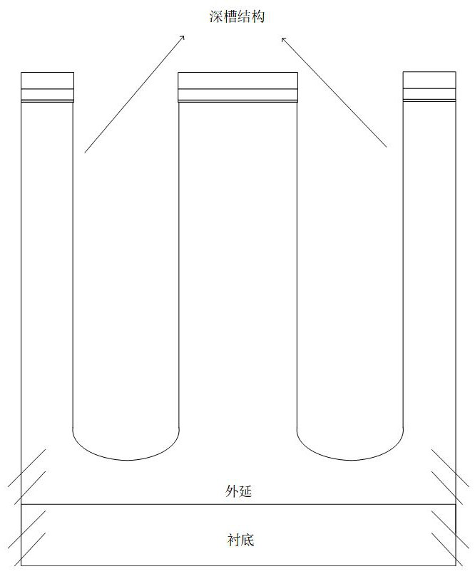
[0050] The invention relates to a method for manufacturing a three-stage oxide layer shielding gate trench MOSFET structure. The method uses a CVD process to fill a deep trench with borosilicate glass BSG material, and then makes the borosilicate glass BSG material in the borosilicate glass BSG material through a thermal process. Boron diffuses into the Si material around the deep trench to form P columns, and changes the BSG concentration and annealing temperature to adjust the height, width and concentration of P columns to achieve charge balance with the N-type epitaxial layer.

[0051] Specifically include the following steps:

[0052] Step 1: grow an N-type epitaxial layer on the surface of the Si substrate, and the thickness of the epitaxial layer is determined according to the source-drain withstand voltage required by the device, ranging from 5 microns to 20 micro...


PUM


Abstract

The invention relates to a manufacturing method of a three-section type oxide layer shielding gate trench MOSFET structure. A source-drain breakdown voltage of a traditional SGT device is controlled by the thickness of an oxide layer, the higher the breakdown voltage is, the thicker the required thickness of the oxide layer is, but in order to obtain lower Rsp, the unit cell size needs to be reduced as much as possible. According to the invention, the deep trench is filled with the borosilicate glass BSG material through a CVD process, boron in the borosilicate glass BSG material is diffused into the Si material on the periphery of the deep trench through a thermal process to form a P column, the BSG concentration and the annealing temperature are changed to adjust the high width and concentration of the P column, and charge balance between the P column and the N-type epitaxial layer is achieved. According to the invention, a thick shielding electrode dielectric layer does not need tobe grown in the trench, the BSG has good high-temperature backflow characteristic and good trench filling capability, and the trench CD can be greatly reduced, so that the unit cell size can be reduced, the same breakdown voltage is realized by adopting an epitaxial wafer with higher doping concentration, and the Rsp of the device is reduced.

Description

technical field [0001] The invention belongs to the technical field of semiconductor power devices, and in particular relates to a method for manufacturing a three-stage oxide layer shielding gate trench MOSFET structure. Background technique [0002] The SGT (Shield-Gate-Trench, shielded gate trench) structure introduces horizontal depletion based on the vertical depletion (P-Body / N-Epi junction) of the traditional trench MOSFET due to its charge coupling effect, making the device The electric field changes from a triangular distribution to an approximately rectangular distribution. In the case of epitaxial specifications with the same doping concentration, the device can obtain a higher breakdown voltage, and this structure is widely used in the field of medium and low voltage power devices. [0003] Figure 15 For the traditional SGT (Shield-Gate-Trench, shielded gate trench) structure, a trench is first formed by etching, and then a shielding electrode dielectric layer ...

Claims


Application Information

Patent Timeline
Patent Type & Authority Applications(China)
IPC IPC(8): H01L29/78H01L21/336H01L29/423H01L29/06
CPCH01L29/0603H01L29/4236H01L29/66477H01L29/78
Inventor 杨乐李铁生楼颖颖李恩求刘琦
Owner XIAN LONTEN RENEWABLE ENERGY TECH
Learn More