Bulk acoustic wave magnetoelectric array antenna and preparation method
An array antenna and bulk acoustic wave technology, applied in the direction of separately powered antenna array, antenna, antenna array, etc., can solve the problems of low gain of a single bulk acoustic wave magnetoelectric antenna, limited application range of radiation gain, small radiation area, etc., to achieve Enhance directivity and radiation gain, prevent mutual interference, and improve the effect of radiation gain
- Summary
- Abstract
- Description
- Claims
- Application Information
AI Technical Summary
Problems solved by technology
Method used
Image
Examples
Embodiment 1
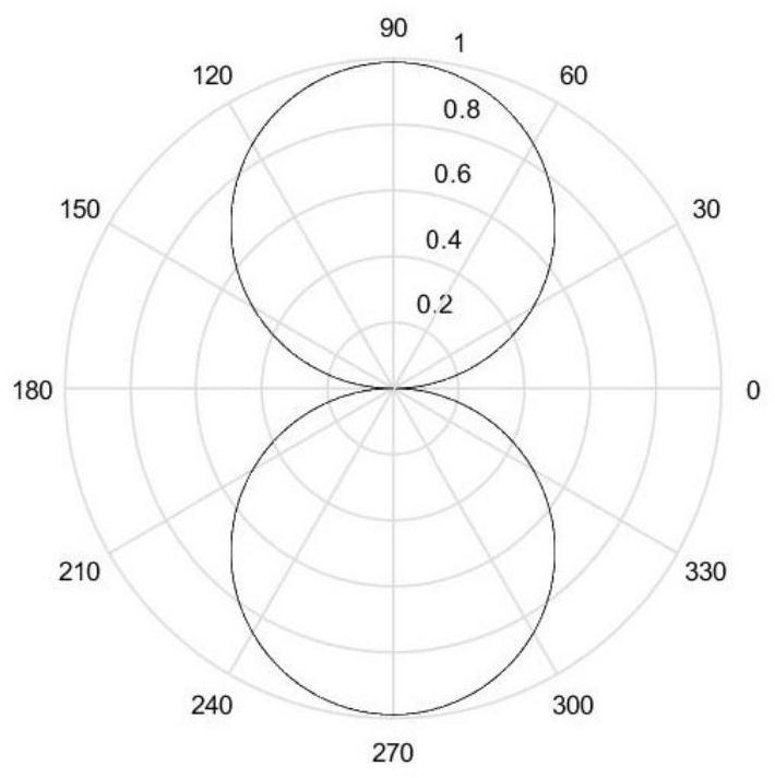
[0037] Such as figure 1 As shown, a bulk acoustic wave magnetoelectric array antenna in this embodiment includes two array elements 9 installed on a silicon base, and the array elements 9 are all bulk acoustic wave magnetoelectric antennas with the same structure; the bulk acoustic wave magnetoelectric antenna consists of The cavity-type bulk acoustic resonator and the magnetostrictive film are compositely composed; the cavity-type bulk acoustic wave resonator includes a silicon substrate 1, an isolation layer 2, an air cavity 3, a seed layer 4, and a lower electrode layer 5 stacked from bottom to top , the piezoelectric layer 6 and the upper electrode layer 7; the magnetostrictive film is made into the magnetostrictive layer 8 and placed on the upper electrode layer 7. The material of the magnetostrictive film is FeGaB with a thickness of 1 μm; the material of the seed layer and the piezoelectric layer are AlN with a thickness of 30nm and 1 μm respectively. The top view of th...
Embodiment 2
[0050] like Figure 4 As shown, a method for preparing a bulk acoustic wave magnetoelectric array antenna in this embodiment includes the following steps:
[0051] S1, using the photolithography process in Figure 5 (a) Two adjacent grooves are etched on the silicon substrate shown in (a), the distance between adjacent grooves is one wavelength, the depth is 1.5 μm, and the surface area is 100 μm×100 μm-200 μm×200 μm; and oxidized by wet oxygen The process forms about 150nm SiO 2 Isolation layer 2, the result is as Figure 5 as shown in (b);
[0052] S2, using magnetron sputtering to fill the two grooves with amorphous silicon as Figure 5 The sacrificial layer shown in (c) has a thickness of about 1.5 μm, and the thickness of the amorphous silicon is higher than the depth of the groove. After that, the surface of the amorphous silicon layer and the isolation layer 2 are smoothed by using a chemical mechanical polishing process. The results are as follows Figure 5 as sho...
PUM
 Abstract
Description
Claims
Application Information
 - R&D
- Intellectual Property
- Life Sciences
- Materials
- Tech Scout
- Unparalleled Data Quality
- Higher Quality Content
- 60% Fewer Hallucinations
Browse by: Latest US Patents, China's latest patents, Technical Efficacy Thesaurus, Application Domain, Technology Topic, Popular Technical Reports.
© 2025 PatSnap. All rights reserved.Legal|Privacy policy|Modern Slavery Act Transparency Statement|Sitemap|About US| Contact US: help@patsnap.com


