Transverse SCR anti-static structure for SOI process and preparation method thereof

An anti-static, lateral technology, applied in circuits, electrical components, electrical solid-state devices, etc., can solve problems such as inability to meet miniaturization requirements, SCR performance impact, and inability to freely choose doping concentration and doping area size.

Pending Publication Date: 2021-03-19
NO 47 INST OF CHINA ELECTRONICS TECH GRP
View PDF0 Cites 1 Cited by
  • Summary
  • Abstract
  • Description
  • Claims
  • Application Information

AI Technical Summary

Problems solved by technology

[0003] With the development of processing technology and the improvement of processing capacity, the size of integrated circuits continues to shrink, and the current mainstream process technology has reached the level of 28nm. Due to the inherent PNPN structure of the SCR structure, the lateral diffusion of impurities, etc., such as figure 1 As shown, the area prepared by the conventional proces

Method used


Image

  • Transverse SCR anti-static structure for SOI process and preparation method thereof
  • Transverse SCR anti-static structure for SOI process and preparation method thereof
  • Transverse SCR anti-static structure for SOI process and preparation method thereof

Examples


Embodiment Construction

[0025] The present invention will be further described in detail below in conjunction with the accompanying drawings and embodiments.

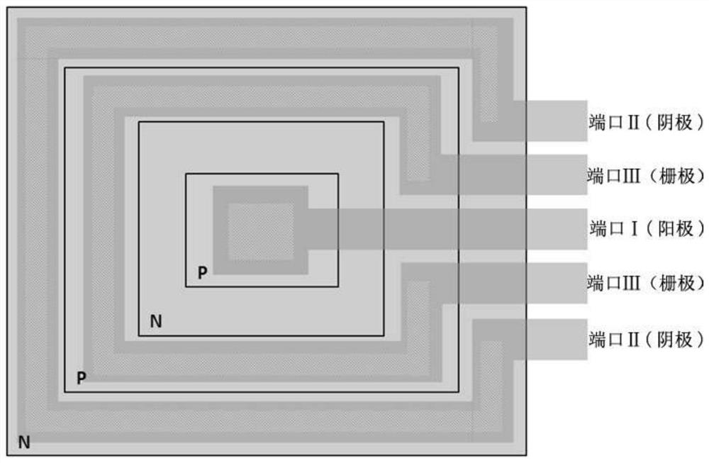
[0026] Such as figure 1 As shown, the traditional SCR antistatic structure mostly adopts a lateral SCR structure, forming N well and P well regions respectively, and then forming N+ and P+ regions by pre-deposition. This preparation method has to consider factors such as lateral diffusion and related The formation of the region depends on the oxidation diffusion preparation process of the circuit. The chip area that needs to be used is relatively large, and the SCR structural parameters or impurity concentration cannot be adjusted under the condition of ensuring the circuit performance, and the process limitation is relatively large.

[0027] Such as figure 2 As shown, the antistatic structure of the SCR of the present invention is distributed in a horizontal PNPN, and the whole is divided into 4 regions, of which the innermost is the P regi...


PUM


Abstract

The invention discloses a transverse SCR anti-static structure for an SOI process and a preparation method thereof, and belongs to the technical field of integrated circuits. The SCR anti-static structure integrally adopts an annular structure, comprises four areas, forms a transverse PNPN structure of the SCR, is led out through metal wiring, can adjust impurity concentration and size according to requirements, adopts deep groove isolation, and can be placed at any position of a circuit. High-energy ion implantation and laser annealing are adopted to achieve accurate control over the doping concentration and the size of a doped region, ion implantation is conducted in two steps, the implantation ranges are 40% and 30% of the thickness of an epitaxial layer respectively, impurity re-diffusion is achieved through a laser annealing process, the process is conducted after other structures of the circuit are formed, a thermal process is not needed, and the function and the performance of the circuit are not influenced; and physical and electrical isolation of the SCR anti-static structure is realized by adopting a deep trench isolation process.

Description

technical field [0001] The invention relates to the technical field of integrated circuits, in particular to a lateral SCR antistatic structure used in SOI technology and a preparation method thereof. Background technique [0002] With the continuous development of integrated circuits, the static electricity generated in the testing, packaging, transportation and other links of integrated circuit chips is the main factor leading to the decline of product reliability. How to design and prepare the antistatic structure of the chip, that is, to meet the antistatic index requirements, At the same time, it is relatively easy to realize, and has become a key topic of research at home and abroad. At present, the more common antistatic structures include diodes, triodes, MOS devices, SCR (silicon controlled silicon), etc., among which the SCR structure is widely used in integrated circuits such as CMOS due to its higher robustness. [0003] With the development of processing techno...

Claims


Application Information

Patent Timeline
IPC IPC(8): H01L27/02H01L27/12H01L21/84
CPCH01L21/84H01L27/0262H01L27/1203
Inventor 吴会利尹自强
Owner NO 47 INST OF CHINA ELECTRONICS TECH GRP
Why Eureka
Try Eureka