Inverted-structure quantum dot light-emitting diode and preparation method thereof
A quantum dot light-emitting, inverted structure technology, applied in semiconductor/solid-state device manufacturing, electrical components, electrical solid-state devices, etc., can solve problems such as difficulty in obtaining an ordered, high-quality thin-film modification layer, and improve charge balance and performance. , the effect of increasing the probability of radiation recombination
- Summary
- Abstract
- Description
- Claims
- Application Information
AI Technical Summary
Problems solved by technology
Method used
Image

Examples
preparation example Construction
[0038] The present invention provides a method for preparing a quantum dot light-emitting diode based on the above-mentioned inverted structure, comprising the following steps:
[0039] Step S1, preparing the substrate;
[0040] Step S2, preparing an electron transport layer on the substrate;
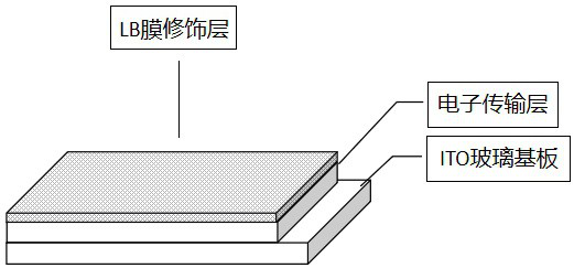
[0041] Step S3, preparing an LB film modification layer on the electron transport layer; the specific preparation method is as follows:
[0042] S31. Dissolving the organic polymer in an organic solvent to form an organic polymer solution;
[0043] S32. Use a micropipette to evenly distribute and drop the organic polymer solution on the subphase / air interface, let it spread automatically, wait for the organic solvent to volatilize for 5-20 minutes, and use the LB film pulling machine to pull to obtain a single layer of orderly organic polymer films;
[0044] S33. Repeat steps S31 and S32 to obtain organic polymer films of different thicknesses, that is, the LB film modification layer...
Embodiment 1
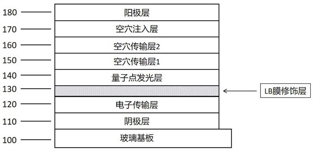
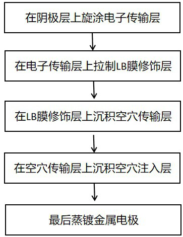
[0053] Such as figure 1 Shown is a schematic structural view of an embodiment of an inverted structure quantum dot light-emitting diode provided by the present invention; the QLED device includes a substrate 100, a cathode layer 110, an electron transport layer 120, an LB film modification layer 130, a quantum dot light-emitting layer 140, a space The hole transport layer 150 , the hole injection layer 170 and the anode layer 180 . Its concrete preparation steps are:
[0054] Step 1: Pretreatment of the ITO glass substrate 100 .
[0055] The substrate 100 is made of glass, the cathode layer 110 is a transparent conductive electrode, and an ITO conductive film prepared by magnetron sputtering; the substrate 100 with ITO is ultrasonically cleaned with deionized water, acetone, and ethanol for 10-20 minutes in sequence, and placed Dry it in a vacuum drying oven for 0.5-1 hour for later use, and perform plasma treatment on the substrate 100 before use;
[0056] Step 2: Preparat...
Embodiment 2
[0070] The preparation process of a quantum dot light-emitting diode with an inverted structure is consistent with that of Example 1, except that a hole transport layer 160 is deposited again on the hole transport layer 150, and all the hole transport layers 150, hole transport Layer 160, hole injection layer 170, and anode layer 180 are all prepared by vacuum evaporation. Its step 1, step 2, step 3, step 4 are identical with embodiment 1, and all the other steps are as follows:
[0071] Step 5: Preparation of the first hole transport layer 150 .
[0072] A hole transport layer 150 is deposited on the quantum dot light-emitting layer 140, the material used is NPB, and the deposition method is an evaporation method. The evaporation rate is controlled to be 1-4 angstroms / second, and the thickness is 10-20nm.
[0073] Step 6: Preparation of the second hole transport layer 160 .
[0074] A hole transport layer 160 is deposited on the first hole transport layer 150, the material...
PUM
| Property | Measurement | Unit |
|---|---|---|
| thickness | aaaaa | aaaaa |
Abstract
Description
Claims
Application Information
 - R&D
- Intellectual Property
- Life Sciences
- Materials
- Tech Scout
- Unparalleled Data Quality
- Higher Quality Content
- 60% Fewer Hallucinations
Browse by: Latest US Patents, China's latest patents, Technical Efficacy Thesaurus, Application Domain, Technology Topic, Popular Technical Reports.
© 2025 PatSnap. All rights reserved.Legal|Privacy policy|Modern Slavery Act Transparency Statement|Sitemap|About US| Contact US: help@patsnap.com