Method for designing and manufacturing blue light Mico-LED chip with inverted structure

A technology of chip design and manufacturing method, which is applied in the direction of semiconductor devices, electrical components, circuits, etc., can solve the problems of large Micro-LED chip spacing, Micro-LED cannot be popularized, and reduce internal quantum efficiency and light extraction efficiency, so as to improve photoelectricity Improvement in performance, light extraction efficiency, reliability and service life

Inactive Publication Date: 2021-03-16
WUHAN UNIV
View PDF6 Cites 3 Cited by
  • Summary
  • Abstract
  • Description
  • Claims
  • Application Information

AI Technical Summary

Problems solved by technology

[0004] At present, Micro-LED has not been popularized, and there are still many technical limitations
Traditional Micro-LED manufacturing uses a deep dry etching process to form electrode through holes to limit the current path, resulting in enhanced non-radiative recombination of electrons and holes on the side walls of the through hole structure, thereby reducing the internal quantum efficiency (IQE), Light extraction efficiency (LEE), at the same time, the Micro-LED chip with a horizontal structure has a larger spacing than the Micro-LED chip with a flip-chip structure, and the display volume is larger, and it is not easy to make miniaturization

Method used


Image

  • Method for designing and manufacturing blue light Mico-LED chip with inverted structure
  • Method for designing and manufacturing blue light Mico-LED chip with inverted structure
  • Method for designing and manufacturing blue light Mico-LED chip with inverted structure

Examples


Embodiment Construction

[0035] The following will clearly and completely describe the technical solutions in the embodiments of the present invention in combination with the embodiments of the present invention. Obviously, the described embodiments are only some of the embodiments of the present invention, not all of them. Based on the embodiments of the present invention, all other embodiments obtained by persons of ordinary skill in the art without creative efforts fall within the protection scope of the present invention.

[0036] It should be noted that, in the case of no conflict, the embodiments of the present invention and the features in the embodiments can be combined with each other.

[0037] The present invention will be further described below in conjunction with specific examples, but not as a limitation of the present invention.

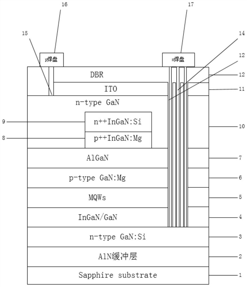
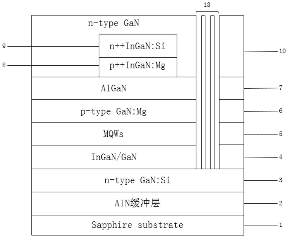
[0038] In this embodiment, the vertical current path in the Micro-LED is limited by the tunnel junction formed between the heavily doped p-GaN and n-GaN, and ...


PUM

PropertyMeasurementUnit
thicknessaaaaaaaaaa
thicknessaaaaaaaaaa
thicknessaaaaaaaaaa

Abstract

The invention belongs to the field of semiconductor light emitters, and particularly relates to a method for designing and manufacturing a blue light Mico-LED chip with an inverted structure, which adopts a tunneling junction formed by heavily doped p + + GaN and n + + GaN to limit a current path, reduces contact resistance, improves Si donor and Mg acceptor concentrations, improves the radiativerecombination rate of electron holes, and improves the internal quantum efficiency and the light extraction efficiency. According to the invention, the Micro-LED with an inverted structure is adopted,ITO / DBR is respectively used as the transparent conductive layer and the current blocking layer, photons emitted by the active region are reflected by the DBR and then are emitted into the air from the sapphire substrate, and the light extraction efficiency is improved. And meanwhile, the requirements that the Micro-LED display is small in size and easy to miniaturize are met. And the Micro-LED chip is designed into an inverted structure, so that the photoelectric property and the thermal stability of the chip are improved.

Description

technical field [0001] The invention belongs to the field of semiconductor light emitters, in particular to a blue light Mico-LED chip with a flip-chip structure. Background technique [0002] Micrometer-sized Light Emitting Diodes (Micro-LED for short) is a new generation of display technology. When the size of LED chips is reduced to tens of microns or even a few microns, they are called Micro-LED chips. Because each pixel of the Micro-LED display can be addressed and individually driven to light up, the micro-display based on the Micro-LED chips of the three primary colors of red, green and blue can display a pixel pitch of micron level, and the imaging effect is excellent, which can realize high-resolution, High contrast, high color saturation, low power consumption, fast response, strong anti-interference ability, etc., have important application value in high-resolution display, visible light communication and other fields. The continuous development and progress of t...

Claims


Application Information

Patent Timeline
Patent Type & Authority Applications(China)
IPC IPC(8): H01L33/32H01L33/14H01L33/44H01L33/64H01L33/00
CPCH01L33/0075H01L33/14H01L33/32H01L33/44H01L33/64
Inventor 周圣军陶国裔万辉
Owner WUHAN UNIV
Why Eureka
Try Eureka