Method for constructing periodic strip domain in ferroelectric film by using pinpoint electric field
A ferroelectric thin film and periodic technology, which is applied in the field of constructing periodic strip domains to achieve the effects of simple design, good stability and efficient preparation
- Summary
- Abstract
- Description
- Claims
- Application Information
AI Technical Summary
Problems solved by technology
Method used
Image
Examples
Embodiment 1
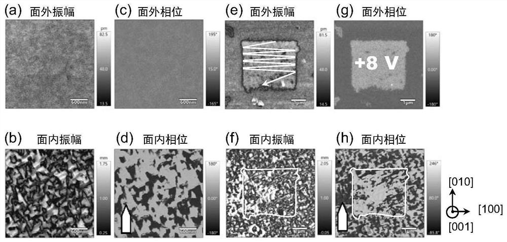
[0046] The selected film corresponds to sample 1 ( figure 2 a, b), below, with image 3 This embodiment will be described in detail in combination.
[0047] According to step S3, the initial state of the ferroelectric thin film is characterized by the vector PFM method, and the out-of-plane ( image 3 a,c) and in-plane ( image 3 b, d) PFM diagrams. From the single contrast of the out-of-plane phase map, it can be seen that the polarization has a unified orientation, and the out-of-plane phase map written in combination with the tip bias (+8V) ( image 3 c), it can be determined that the out-of-plane initial polarization of the film points upward uniformly, indicating that the growth rate of the bottom electrode is slightly faster under the condition of low oxygen pressure, because SrRuO 3 Generally considered to have metallic conductivity, the spontaneous polarization direction of the ferroelectric layer grown on it should point downward. From the in-plane PFM phase dia...
Embodiment 2
[0049] The selected film corresponds to sample 2 ( figure 2 c,d), below, with Figure 4 , Figure 5 This embodiment will be described in detail in combination.
[0050] Determine the relative orientation of the sample to the probe cantilever, e.g. Figure 4 As shown in a, the eight polarizations of the corresponding lattice point at Figure 4 given in d. According to step S4, a rectangular pattern is written in the film, the tip bias voltage is -4V, and the scanning direction of the tip is as follows: Figure 4 Shown by the white broken line in e. The vector PFM method is used to characterize the ferroelectric thin film, and the read area is much larger than the write area, in order to give the spontaneous growth ( Figure 4 The domain structure (step S3) of the region outside the middle white rectangle frame); the region outside the rectangle frame, the out-of-plane PFM phase map ( Figure 4 e) is the contrast between light and dark. It can be seen that the polarizati...
PUM
| Property | Measurement | Unit |
|---|---|---|
| thickness | aaaaa | aaaaa |
| thickness | aaaaa | aaaaa |
| size | aaaaa | aaaaa |
Abstract
Description
Claims
Application Information
 - R&D
- Intellectual Property
- Life Sciences
- Materials
- Tech Scout
- Unparalleled Data Quality
- Higher Quality Content
- 60% Fewer Hallucinations
Browse by: Latest US Patents, China's latest patents, Technical Efficacy Thesaurus, Application Domain, Technology Topic, Popular Technical Reports.
© 2025 PatSnap. All rights reserved.Legal|Privacy policy|Modern Slavery Act Transparency Statement|Sitemap|About US| Contact US: help@patsnap.com


