


Quick Research
Generate reliable direction feasibility study reports for your R&D in just a few steps.

Technical Q&A
Discover and master advanced knowledge NOW. Basics, ideas, possibilities, all at once.

Find Solutions
As an expert in R&D theories, this can generate solutions to your technical problems instantly.

Evaluate Feasibility
Analyze your overall solution with one click, know your potential R&D risks in advance.

Monitor Landscape
Get weekly tech updates, stay abreast of the latest tech innovations and key insights.
Chip packaging structure and vehicle
A chip packaging structure and chip technology, applied in electrical components, electrical solid devices, circuits, etc., can solve the problems of increased dynamic loss, increased parasitic inductance inside the device or module, and large temperature rise, so as to reduce the temperature rise under operating conditions and improve the overall performance, the effect of reducing parasitic inductance
- Summary
- Abstract
- Description
- Claims
- Application Information
AI Technical Summary
Problems solved by technology
Method used
Image

Examples
Embodiment 1
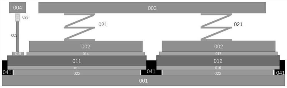
[0030] A chip packaging structure, including a first conductive and thermally conductive member 001, a second conductive and thermally conductive member 002, and a first conductive and thermally conductive elastic member 022, the chip is located between the first conductive and thermally conductive member 001 and the second conductive and thermally conductive member 002, the The first thermally conductive elastic member 022 is located between the first thermally conductive member 001 and the chip.
[0031] The chip packaging structure further includes an insulating frame 041, and the insulating frame 041 is arranged on the side of the first conductive and heat-conducting member 001 facing the chip;
[0032] The chips are arranged on the insulating frame 041 .
[0033] The chip package structure further includes a second conductive and thermally conductive elastic member 021 and a third conductive and thermally conductive member 003, the second conductive and thermally conducti...
Embodiment 2
[0056] A chip packaging structure, including a first conductive and thermally conductive member 001, a second conductive and thermally conductive member 002, and a first conductive and thermally conductive elastic member 022, the chip is located between the first conductive and thermally conductive member 001 and the second conductive and thermally conductive member 002, the The first thermally conductive elastic member 022 is located between the first thermally conductive member 001 and the chip.
[0057] The chip packaging structure further includes an insulating frame 041, and the insulating frame 041 is arranged on the side of the first conductive and heat-conducting member 001 facing the chip;
[0058] The chips are arranged on the insulating frame 041 .
[0059] The chip package structure further includes a second conductive and thermally conductive elastic member 021 and a third conductive and thermally conductive member 003, the second conductive and thermally conducti...
Embodiment 3
[0079] A chip packaging structure, the same as the second embodiment will not be repeated, the chip is a diode chip 012;
[0080] in
[0081] The material of the diode chip 012 is but not limited to silicon or silicon carbide, and the diode chip 012 includes a chip front metal system 017 of the diode chip and a chip back metal system 016 of the diode chip.
PUM
 Abstract
Description
Claims
Application Information
 - R&D Engineer
- R&D Manager
- IP Professional
- Industry Leading Data Capabilities
- Powerful AI technology
- Patent DNA Extraction
Browse by: Latest US Patents, China's latest patents, Technical Efficacy Thesaurus, Application Domain, Technology Topic, Popular Technical Reports.
© 2024 PatSnap. All rights reserved.Legal|Privacy policy|Modern Slavery Act Transparency Statement|Sitemap|About US| Contact US: help@patsnap.com