Laser etching device for MEMS probe

A technology of laser etching and probe, which is applied in the direction of microstructure devices, laser welding equipment, manufacturing microstructure devices, etc. It can solve the problems of complex probe structure, high cost, high production cost of small-sized high-precision probes, etc.

Active Publication Date: 2021-02-23
强一半导体(苏州)股份有限公司
View PDF12 Cites 1 Cited by
  • Summary
  • Abstract
  • Description
  • Claims
  • Application Information

AI Technical Summary

Problems solved by technology

However, in order to realize the preparation of smaller-sized probes and ensure higher etching precision in this process, the cost of process equipment used will increase exponentially. Therefore, the production cost of small-sized high-precision probes is extremely high
[0011] In response to the above problems, a probe preparation process based on laser etching method has emerged. This preparation process can effectively solve the environmental protection problems of the bottom-up electroplating method and the top-down photolithography method. high cost problem
[0012] As the size of the probes becomes smaller and smaller, the precision of laser etching is required to be higher and higher. At the same time, with the continuous emergence of the demand for special probe cards, the structure of the corresponding probes becomes more and more complex. The corresponding laser ablation pattern It also becomes irregular, which brings more and more challenges to the etching. In order to adapt to this change, a laser etching device with high precision and continuous adjustment of the spacing is urgently needed. However, through the existing data With the understanding of equipment and equipment, a general-purpose laser etching equipment, method and key technology that can realize the above functions have not been found.

Method used


Image

  • Laser etching device for MEMS probe
  • Laser etching device for MEMS probe
  • Laser etching device for MEMS probe

Examples


specific Embodiment approach 1

[0135] The following is the specific implementation of the MEMS probe laser etching device of the present invention.

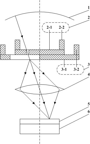
[0136] The structure schematic diagram of MEMS probe laser etching device under this embodiment is as follows figure 1 As shown, in the MEMS probe laser etching device, according to the light propagation direction, an arc light source 1, a spiral channel plate 2, a straight channel plate 3, an objective lens 4, a single crystal silicon wafer 5 and a four-dimensional station 6;

[0137] Each point of said arc light source 1 is identical to object lens 4 center distances, and promptly the shape of arc light source 1 is the circular arc shape taking object lens 4 center as the center; The line connecting the center is vertical;

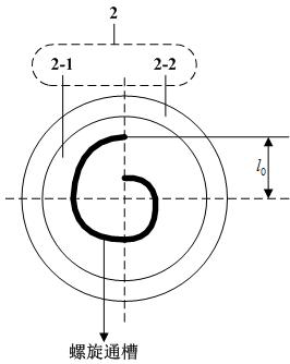
[0138] The structural representation of the spiral channel plate 2 is as follows: figure 2 As shown, it includes a first bottom plate 2-1 with a spiral groove and a first side 2-2 with a circular cross-section. The outer surface of t...

specific Embodiment approach 2

[0146] The following is the specific implementation of the MEMS probe laser etching device of the present invention.

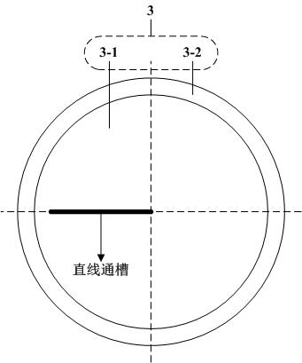
[0147] The MEMS probe laser etching device under this embodiment is further defined on the basis of Embodiment 1: a scraper is arranged around the linear through groove of the second bottom plate 3-1, and a scraper is arranged on the upper surface of the second bottom plate 3-1. There are a plurality of annular grooves concentric with the second bottom plate 3-1, and the annular grooves start and stop at the scrapers around the straight through groove; the upper surface of the second bottom plate 3-1 is also provided with linear grooves in the radial direction, and the annular grooves It communicates with the linear groove crosswise, and the annular groove and the linear groove are filled with lubricating oil, such as Figure 5 As shown, the lubricating oil drips from between the first side 2-2 and the second side 3-2.

specific Embodiment approach 3

[0149] The following is the specific implementation of the MEMS probe laser etching device of the present invention.

[0150] The MEMS probe laser etching device under the present embodiment is further limited on the basis of the specific embodiment one or the specific embodiment two: the structure of the MEMS probe laser etching device, such as Figure 6 As shown, the first side 2 - 2 is externally meshed with a gear 7 , and the rotation of the gear is controlled by a motor 8 , the motor 8 is connected to a controller 9 , and the controller 9 is connected to the four-dimensional table 6 .


PUM


Abstract

The invention discloses a laser etching device for an MEMS probe, which belongs to the technical field of semiconductor processing and testing. The device is sequentially equipped with an arc-shaped light source, a spiral through slot plate, a linear through slot plate, an objective lens, a single crystal silicon wafer and a four-dimensional table in a light propagation direction, wherein the distance from each point of the arc-shaped light source to the center of the objective lens is the same, a tangent line is perpendicular to a connecting point from the point to the center of the objectivelens; the spiral through slot plate comprises a first bottom plate with a spiral through slot and a first side with a circular ring shaped section; the linear through slot plate comprises a second bottom plate with a linear through slot and a second side with a circular ring shaped section; the upper surface of the second bottom plate clings to the lower surface of the first bottom plate; the upper surface of the single crystal silicon wafer and the second bottom plate are separately positioned on the mirror surface and the objective surface of the objective lens; and the single crystal silicon wafer is subjected to three-dimensional translation and one-dimensional rotation. The laser etching device for the MEMS probe is matched with a laser etching method for the MEMS probe, so that etching precision is higher, and an etching spacing can be continuously adjusted.

Description

technical field [0001] The invention relates to a MEMS probe laser etching device, which belongs to the technical field of semiconductor processing and testing. Background technique [0002] The probe card is a test interface used to test the bare core. By directly contacting the probes on the probe card with the pads or bumps on the IC chip, the IC chip signal is drawn out, and then cooperates with the test instrument to write to the IC chip. Input the test signal, and then realize the test before IC chip packaging. [0003] One of the core structures of the probe card is the probe. At present, there are two methods of making probes: bottom-up and top-down. [0004] Bottom-up plating method: [0005] CN201010000429.2, a microprobe structure and its manufacturing method, using the lithography, electroplating, planarization and etching technologies of the semiconductor manufacturing process, and replacing the electroplating second sacrificial layer metal with polymers, on ...

Claims


Application Information

Patent Timeline
IPC IPC(8): B23K26/046B23K26/362B81B7/02B81C1/00H01L21/66
CPCB23K26/362B23K26/046B81C1/00523B81B7/02H01L22/14B81C2201/013
Inventor 于海超周明
Owner 强一半导体(苏州)股份有限公司
Why Eureka
Try Eureka