Eureka AIR delivers breakthrough ideas for toughest innovation challenges, trusted by R&D personnel around the world.

Method for assembling quantum dot laser on planar superlattice nanowire

A superlattice and nanowire technology, applied in the field of semiconductor devices, can solve the problem that colloidal quantum dots cannot be positioned accurately, and achieve the effect of expanding the scope of application

Active Publication Date: 2021-02-12
NANJING UNIV
View PDF6 Cites 2 Cited by
  • Summary
  • Abstract
  • Description
  • Claims
  • Application Information

AI Technical Summary

Problems solved by technology

However, the colloidal quantum dots prepared by this method cannot be positioned accurately, and scanning probes are needed

Method used


Image

  • Method for assembling quantum dot laser on planar superlattice nanowire
  • Method for assembling quantum dot laser on planar superlattice nanowire

Examples


Embodiment Construction

[0027] The present invention will be further explained below in conjunction with the accompanying drawings and specific embodiments.

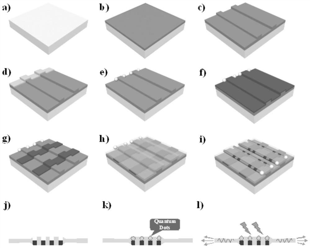
[0028] Such as figure 1 As shown, this embodiment provides a method for assembling a quantum dot laser on a planar superlattice nanowire, which specifically includes the following steps:

[0029] 1) Deposit a layer of insulating medium after pretreatment of the substrate material

[0030] Such as figure 1 (a), figure 1 As shown in (b): the substrate in this embodiment can be crystalline silicon, glass, aluminum foil, silicon nitride, silicon oxide, silicon carbide, sapphire, PI (polyimide) or PET (polyterephthalic acid) Plastic), using PECVD or PVD process to deposit a layer of 200~1000nm thick insulating dielectric layer.

[0031] Preferably, in this embodiment, an insulating dielectric layer with a thickness of 100-600 nm is deposited, and the material of the insulating dielectric layer is silicon oxide or silicon nitride.

[0032] ) Etc...


PUM

PropertyMeasurementUnit
Thicknessaaaaaaaaaa
Covering thicknessaaaaaaaaaa
Sizeaaaaaaaaaa

Abstract

The invention discloses a method for assembling a quantum dot laser on a planar superlattice nanowire, and the method comprises the steps: carrying out the spin coating of a quantum dot solution on the etched superlattice nanowire, and obtaining a superlattice nanowire embedded with quantum dots after drying; employing ultraviolet light or infrared light for irradiating quantum dots embedded intosuperlattice nanowires so that the quantum dots emit light, taking the silicon nanowires at the two ends of the superlattice structure as optical waveguides, locating quantum dot optical signals and transmitting the signals through the nanowire guided wave effect, and testing the light collection and transmission effects of the nanowires of the superlattice structure.

Description

technical field [0001] The invention relates to a method for assembling a quantum dot laser on a plane superlattice nanowire, belonging to the technical field of semiconductor devices. Background technique [0002] Semiconductor nanowires are key building blocks for developing next-generation high-performance micro-nanoelectronic logic, sensing, and display applications. In order to be more compatible with the planar electronic process and realize positioning integration, the inventors of the present application proposed a method for controlling the growth morphology and composition of planar silicon germanium and related nanowires supplied by heterogeneous stacked amorphous films : Among them, a composite laminated amorphous silicon and amorphous germanium layer is used as the precursor supply layer, and the amorphous layer is absorbed by low-melting metal indium and tin nanoparticles to directly grow germanium-silicon heterogeneous self-nested nanowires on a planar substra...

Claims


Application Information

Patent Timeline
IPC IPC(8): H01S5/34H01S5/20H01S5/30B82Y30/00B82Y40/00
CPCH01S5/3412H01S5/3018H01S5/20B82Y40/00B82Y30/00H01S2304/00
Inventor 余林蔚刘帅帅王军转
Owner NANJING UNIV
Why Eureka
Eureka Blog
Learn More