


Quick Research
Generate reliable direction feasibility study reports for your R&D in just a few steps.

Technical Q&A
Discover and master advanced knowledge NOW. Basics, ideas, possibilities, all at once.

Find Solutions
As an expert in R&D theories, this can generate solutions to your technical problems instantly.

Evaluate Feasibility
Analyze your overall solution with one click, know your potential R&D risks in advance.

Monitor Landscape
Get weekly tech updates, stay abreast of the latest tech innovations and key insights.
High-reliability thermoelectric device and preparation method
A thermoelectric device and reliability technology, applied in the manufacture/processing of thermoelectric devices, thermoelectric device components, etc., can solve problems such as cracks and affect the performance of thermoelectric materials, and achieve the effect of reducing crack damage and improving reliability.
- Summary
- Abstract
- Description
- Claims
- Application Information
AI Technical Summary
Problems solved by technology
Method used
Image

Examples
preparation example Construction
[0026] A method for preparing a high-reliability thermoelectric device comprises the following steps:
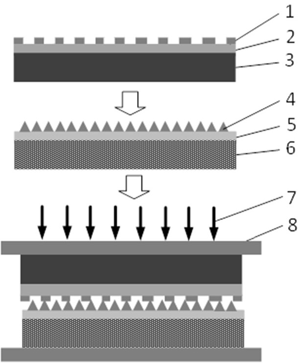
[0027] (1) First, slice the thermoelectric material device into a thermoelectric chip 3, clean the bonding surface of the thermoelectric chip 3 by using a standard RCA process, and sputter a nickel metal layer 2 on the package connection surface of the thermoelectric chip 3. The nickel The thickness of the metal layer 2 is 1-2 microns, so as to prevent the copper atoms in the copper metal layer 5 of the copper-clad ceramic substrate 6 from diffusing into the thermoelectric material device.
[0028] (2) Corroding the surface of the sputtered nickel metal layer 2 with a dealloying method to prepare a metal nickel layer 1 with a nanopore structure, the thickness of the metal nickel layer 1 with a nanopore structure is 200-500 nanometers, and its pore diameter is 50 -200 nanometers, with a porosity greater than 60%, use it as a bonding surface for packaging and interconnection, ...
Embodiment 1
[0035] Such as figure 1 As shown, the present invention is a low-temperature bonding method for integrated packaging, including:
[0036] (1) First, the electrothermal material device is cut into several thermoelectric chips 3, the bonding surface of the thermoelectric chips 3 is cleaned by a standard RCA process, and then a nickel metal layer 2 with a thickness of 1 micron is deposited on the substrate by a sputtering process, Finally, on the nickel metal layer 2, a metal nickel layer 1 with a nanopore structure is prepared by a dealloying method.
[0037]The preparation method of the metal nickel layer 1 with a nanopore structure is as follows: firstly, the thermoelectric chip 3 with the nickel metal layer 2 is placed in HCl solution for cleaning, the concentration of the HCl solution is 5%, and the cleaning time is 1 minute, which is used to remove the electric heat. The oxide on the surface of the nickel metal layer 2 of the wafer 3, after that, the thermoelectric chip 3 ...
Embodiment 2
[0043] Such as figure 1 As shown, the present invention is used for the low-temperature bonding method of integrated package, comprises the following steps:
[0044] (1) The electrothermal material device is cut into several thermoelectric chips 3, and the bonding surface of the thermoelectric chips 3 is cleaned by standard RCA process, and then a nickel metal layer 2 is deposited on the substrate by a sputtering process, and the thickness of the nickel metal layer 2 is Two microns, and finally the metal nickel layer 1 with a nanopore structure is prepared by corrosion on the surface of the metal nickel layer 2 by dealloying method.
[0045] The method for preparing the metal nickel layer 1 with a nanopore structure is as follows: the thermoelectric wafer 3 that has been sputtered with the nickel metal layer 2 is placed in a hydrochloric acid solution for cleaning, the concentration of the hydrochloric acid solution is 5%, and the cleaning time is 1 minute for removing The su...
PUM
| Property | Measurement | Unit |
|---|---|---|
| Aperture | aaaaa | aaaaa |
| Cone base diameter | aaaaa | aaaaa |
| Thickness | aaaaa | aaaaa |
Abstract
Description
Claims
Application Information
 - R&D Engineer
- R&D Manager
- IP Professional
- Industry Leading Data Capabilities
- Powerful AI technology
- Patent DNA Extraction
Browse by: Latest US Patents, China's latest patents, Technical Efficacy Thesaurus, Application Domain, Technology Topic, Popular Technical Reports.
© 2024 PatSnap. All rights reserved.Legal|Privacy policy|Modern Slavery Act Transparency Statement|Sitemap|About US| Contact US: help@patsnap.com