
A VLSI Database and Design Method Based on Memory Pool

A large-scale integrated circuit and memory pool technology, applied in CAD circuit design, electrical digital data processing, program control design, etc., can solve the problem that the overall performance of the application program is greatly affected, user-defined data cannot be carried, and information or accuracy is lost and other issues to achieve the effect of eliminating complex dependencies, facilitating search, and responding quickly

Active Publication Date: 2021-03-23
南京集成电路设计服务产业创新中心有限公司
View PDF6 Cites 0 Cited by
  • Summary
  • Abstract
  • Description
  • Claims
  • Application Information

AI Technical Summary

Problems solved by technology

How to ensure that the data is completely transmitted without data loss. When exporting and importing files, even within the scope supported by the standard, information or accuracy will be lost
In addition to the data supported by the standard, user-defined data cannot be carried to the next tool
In addition, there are artificial barriers set by different EDA manufacturers, such as not supporting the data of other manufacturers' tools, especially the data of rival manufacturers
This directly makes switching between different tools extremely inconvenient or even impossible
[0004] The application and release of memory have a great impact on the overall performance of an application, and even become the bottleneck of an application in many cases

Method used


Image

  • A VLSI Database and Design Method Based on Memory Pool
  • A VLSI Database and Design Method Based on Memory Pool
  • A VLSI Database and Design Method Based on Memory Pool

Examples


Embodiment 1

[0053] figure 1 It is a schematic diagram of the VLSI database structure based on the memory pool according to the present invention, such as figure 1 As shown, the memory pool-based VLSI database of the present invention includes a memory pool manager 10, a memory page manager 20, a memory block 30, a memory page 40, a free object list 50, and a data object identifier 60, in,

[0054] The memory pool manager 10 is configured to manage the entire memory pool.

[0055] In the embodiment of the present invention, it consists of a memory pool manager (MemPool), several memory page managers (MemPagePool), several memory chunks (MemChunk) and several memory pages (MemPage). The memory pool manager includes memory pools, which are relatively independent, and different memory pools correspond to different design modules in the chip design. But they are all in the container of the memory pool manager, and correspond to specific chip modules one by one.

[0056] The memory page man...

Embodiment 2

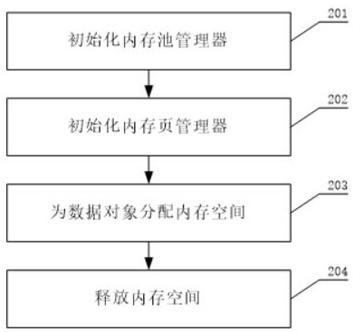
[0067] image 3 For the VLSI database design method flow chart based on the memory pool of the present invention, reference will be made below image 3 , to describe in detail the VLSI database design method based on the memory pool of the present invention.

[0068] First, in step 201, the memory pool manager 10 is initialized.

[0069] In the embodiment of the present invention, the memory pool manager 10 allocates an array space for storing pointers of different memory pools, and at the same time generates a table for mapping the memory pools and circuit design modules.

[0070] In the embodiment of the present invention, after the initialization of the memory pool manager is completed, the program can operate on the circuit design module.

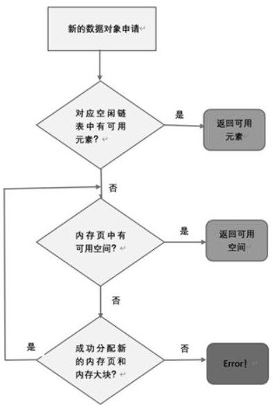
[0071] In the embodiment of the present invention, for a new design module, a new memory pool needs to be allocated for organizing the memory space of the data objects inside it.

[0072] In the embodiment of the present invention, t...

Embodiment 3

[0084] In an embodiment of the present invention, there is also provided an electronic device, including a memory and a processor, wherein a computer program is stored in the memory, and the processor is configured to run the computer program to execute the above memory pool-based The steps of VLSI database design method.


PUM


Abstract

A VLSI database based on a memory pool, including a memory pool manager, a memory page manager, a memory block, a memory page, a free object linked list, and a data object identifier, wherein the memory pool manager uses The memory page manager is used to manage the memory page manager; the memory page manager is used to organize the memory space of the design data object; the memory block is used to allocate to the database for object operation space; the memory page is used to allocate The data object; the free object linked list is used to manage and save the released memory space through the memory page manager; the data object identifier is used as the unique identifier of each data object allocated space. Through the management of the memory pool, the present invention enables the memory allocation and storage reading of the database to have fast response and high-efficiency space utilization, thereby supporting the high requirements for data in VLSI design.

Description

technical field [0001] The invention relates to the field of integrated circuit design automation, in particular to a database design method in EDA tools. Background technique [0002] With the rapid development of the semiconductor industry, the characteristic size of the chip is getting smaller and smaller, and the number of transistors embedded in the chip is also increasing exponentially. Continuous shortening, chip design is facing unprecedented challenges. In order to ensure high-quality, high-reliability products, complete design closure and achieve product function goals within the specified time, the chip design industry increasingly relies on excellent design software. Internationally, the three giants of Cadence, Synopsys, and Mentor under Siemens each have a wide variety of design tools and their own proprietary databases. At the same time, they also support standard format data such as Verilog, LEF / DEF, and Liberty. Input and output, etc. There is also the Op...

Claims


Application Information

Patent Timeline
Patent Type & Authority Patents(China)
IPC IPC(8): G06F9/50G06F30/32
CPCG06F9/5016G06F9/5022G06F30/32
Inventor 陈刚
Owner 南京集成电路设计服务产业创新中心有限公司
Learn More