FPGA high-performance interconnection circuit

A high-performance, circuit technology, applied in multiple input and output pulse circuits, electrical components, electronic switches, etc., can solve the problems of large chip area, limited power consumption improvement of interconnected circuits, large area, etc., and achieve superior performance.

Pending Publication Date: 2021-01-15
CHENGDU SINO MICROELECTRONICS TECH CO LTD
View PDF6 Cites 0 Cited by
  • Summary
  • Abstract
  • Description
  • Claims
  • Application Information

AI Technical Summary

Problems solved by technology

[0003] The traditional interconnection circuit uses the transmission gate as the selector of the MUX, and its area is relatively large, which makes the chip area of ​​the entire FPGA relatively large.
In addition, even if the MOS single-tube design is adopted, the power consumption of the interconnection circuit is still limited.

Method used


Image

  • FPGA high-performance interconnection circuit
  • FPGA high-performance interconnection circuit
  • FPGA high-performance interconnection circuit

Examples


Embodiment

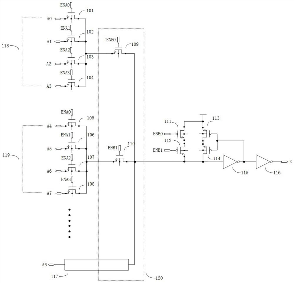
[0031] For ease of reading, the "device referred to by 101" is abbreviated as "101" hereinafter, and the other symbols are the same.

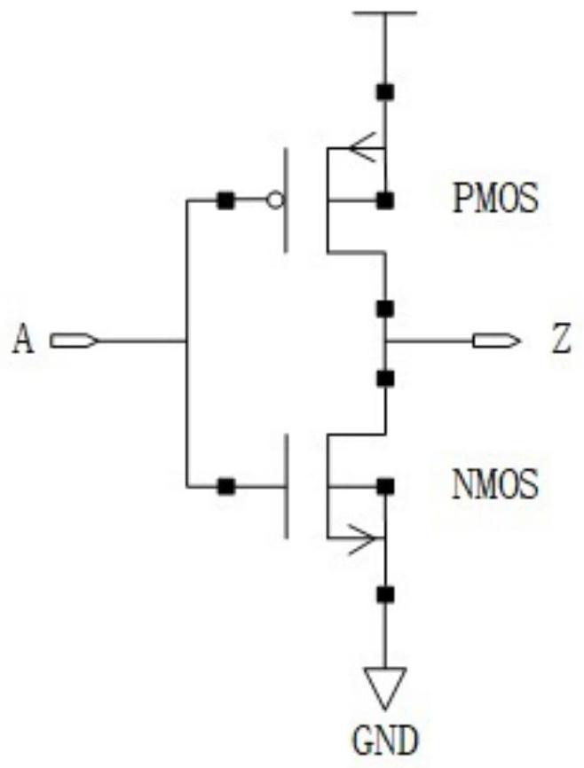
[0032] figure 1 118 and 119 are two sets of the same 4-select-one MUX, and the device types are all NMOS transistors. The gate terminals of 101 and 105, 102 and 106, 103 and 107, 104 and 108 are controlled by the same SRAM; 120 is the first Secondary MUX, the device type is also NMOS transistor, 111 and 112 are pull-up PMOS transistors, of which 109 and 111, the gate terminals of 110 and 112 come from the opposite output of the same SRAM; 113~116 are level recovery circuits, 113 and 112 114 is a PMOS tube, and the inverter structure in the level restoration circuit is composed of image 3 shown. The MUX of this circuit can be expanded.

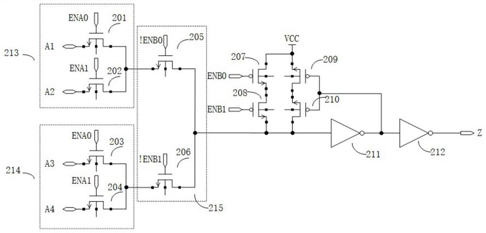
[0033] figure 2 It is the most basic circuit structure of the present invention (two-stage 4 select one MUX), 213 and 214 are two groups of the same 2 select one MUX, the device type is NMOS, and the gate...


PUM


Abstract

The invention discloses an FPGA high-performance interconnection circuit, and relates to an integrated circuit technology. The circuit comprises i secondary NMOS tubes connected in parallel, wherein the output end of each secondary switch NMOS tube is connected to a common reference point; the input end of each secondary NMOS transistor is connected with a primary NMOS transistor group, the primary NMOS transistor group is composed of m primary NMOS transistors which are connected in parallel, the output end of each primary NMOS transistor in the same primary NMOS transistor group is connectedwith the corresponding secondary NMOS transistor, and the input end of each primary NMOS transistor in the same primary NMOS transistor group is used as the input end of the interconnection circuit;in each primary NMOS tube group, the primary NMOS tubes with the same serial number are controlled by the same primary SRAM unit, and each secondary NMOS tube is connected to the corresponding secondary SRAM; wherein the common reference point is connected to the output end through the pull-up circuit and the level recovery circuit, and i and m are integers greater than 1. According to the invention, the performance of the interconnection circuit in the aspects of area, power consumption, speed and signal integrity is more excellent.

Description

technical field [0001] The present invention relates to integrated circuit technology. Background technique [0002] Since the advent of FPGA, while its capacity has been continuously expanded, the interconnection circuit (i.e., FPGA architecture) has also gradually evolved. In the initial period of small-scale FPGAs, designers paid more attention to the design and optimization of logic units. As interconnect circuits account for an increasing share of the performance of large-scale FPGA chips, designers have begun to explore different types of interconnect circuit development. It needs to be considered that the architectural parameters are continuously increasing, forming an FPGA architecture design space with exponentially increasing capacity. Efficiently selecting an optimized architecture that satisfies design specifications from a huge architecture design space is the key to ensuring the rapid availability of FPGAs. [0003] The traditional interconnection circuit use...

Claims


Application Information

Patent Timeline
Patent Type & Authority Applications(China)
IPC IPC(8): H03K5/22H03K17/22
CPCH03K5/22H03K17/22
Inventor 王玉嫣刘云搏丛伟林段清华余梅
Owner CHENGDU SINO MICROELECTRONICS TECH CO LTD
Why Eureka
Try Eureka