
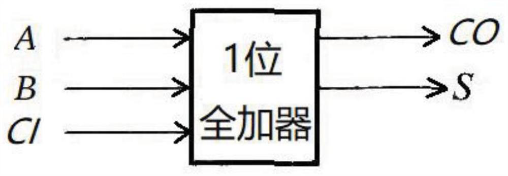
CMOS full adder and multi-bit full adder

A full adder and potential technology, applied in the field of multi-bit full adders, can solve the problems of reduced speed of the operation unit and cannot work normally, and achieve the effect of reducing the rise and improving the speed of the circuit

Pending Publication Date: 2020-12-22
SEMICON MFG INT (SHANGHAI) CORP +1
View PDF0 Cites 1 Cited by
  • Summary
  • Abstract
  • Description
  • Claims
  • Application Information

AI Technical Summary

Problems solved by technology

However, under the near-threshold voltage, the speed of many computing units in the circuit will be greatly reduced, or even fail to work properly.

Method used


Image

  • CMOS full adder and multi-bit full adder
  • CMOS full adder and multi-bit full adder
  • CMOS full adder and multi-bit full adder

Examples


Embodiment Construction

[0036] The specific implementation manners of the present application will be further described in detail below in conjunction with the drawings and embodiments. The following examples are used to illustrate the present application, but not to limit the scope of the present application.

[0037] Exemplary implementations of the present application will be described below with reference to the accompanying drawings. In the interest of clarity and conciseness, not all features of an actual implementation are described in this specification. Here, it should also be noted that, in order to avoid obscuring the application due to unnecessary details, only the device structure and / or processing steps closely related to the solution according to the application are shown in the drawings, and the Other details that are not relevant to this application are included.

[0038] First, the technical terms involved in this application are explained. PMOSFET stands for P-channel Metal Oxid...


PUM


Abstract

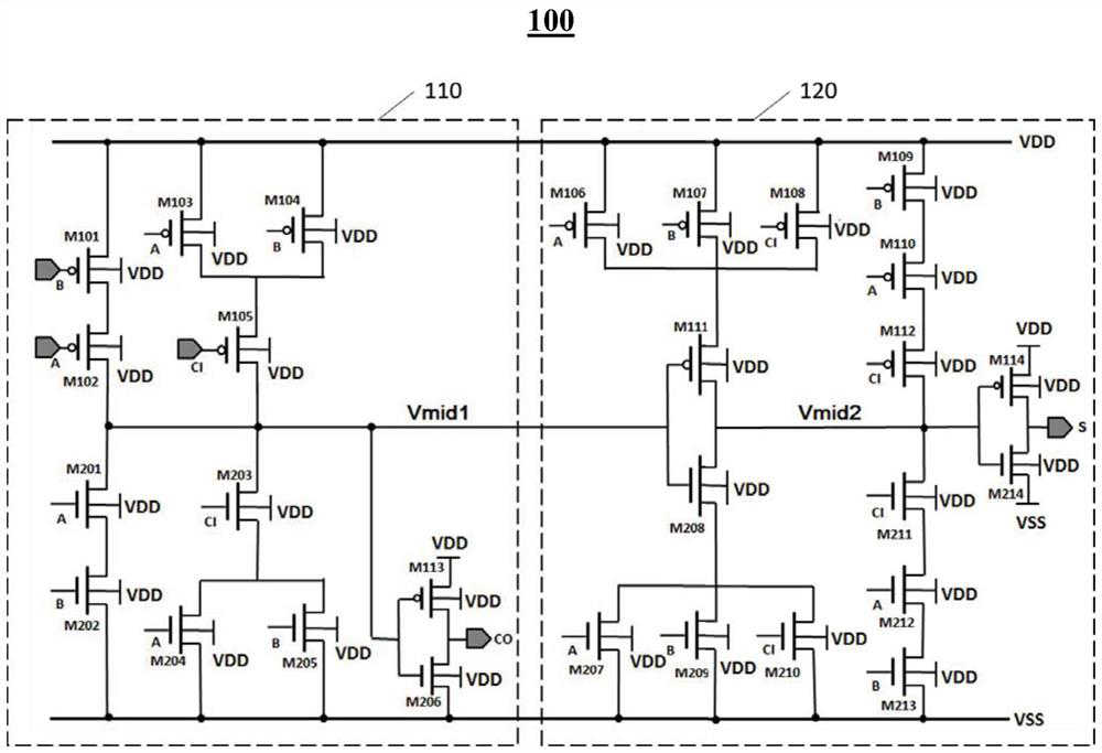
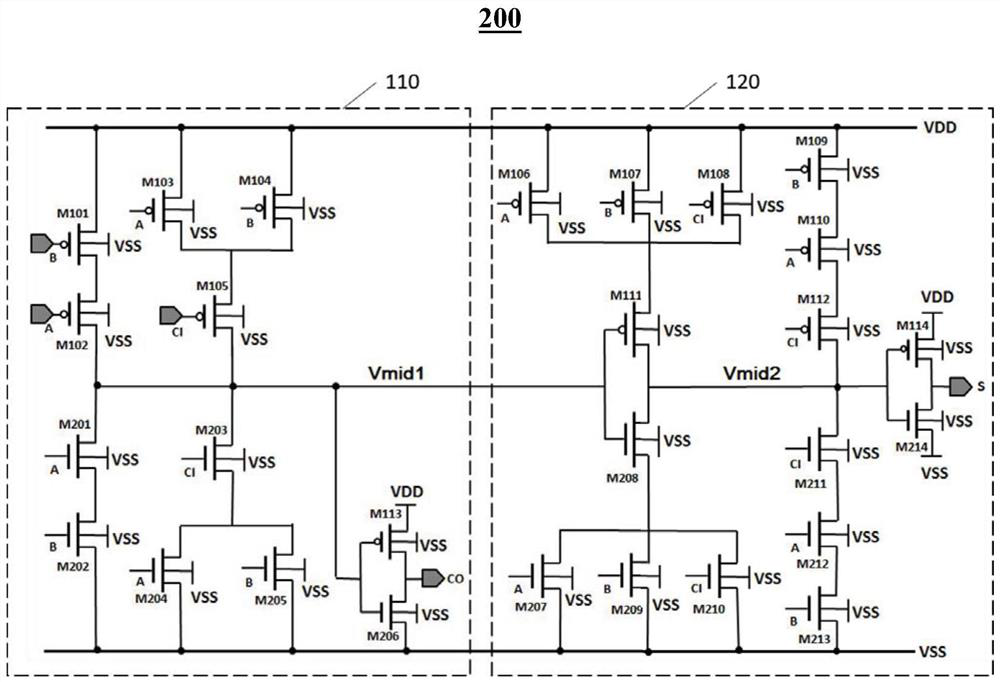
The invention discloses a CMOS full adder. The CMOS full adder comprises more than one PMOS field effect transistor, more than one NMOS field effect transistor and a connecting circuit. The connectingcircuit is used for connecting the more than one PMOS field effect transistor and the more than one NMOS field effect transistor. The connecting circuit is configured to reduce a threshold voltage ofat least one of the more than one PMOS field effect transistor and the more than one NMOS field effect transistor. The invention further discloses a multi-bit full adder. The multi-bit full adder comprises a plurality of CMOS full adders. The CMOS full adder and the multi-bit full adder can effectively reduce the ascending, descending and propagation delay conditions of the device, thereby improving the circuit speed.

Description

technical field [0001] The present application relates to the field of adders, in particular to a CMOS full adder based on substrate bias and a multi-bit full adder composed of multiple CMOS full adders. Background technique [0002] With the development of Internet of Things technology, low power consumption circuit design has become the focus of research. One of the effective ways to reduce power consumption is to reduce the operating voltage of the circuit to near the near-threshold, thus forming a near-threshold circuit. But at a near-threshold voltage, the speed of many computing units in the circuit will be greatly reduced, or even fail to work properly. [0003] In the development of large-scale integrated circuits, data computing has always played an important role. The addition operation (including summation, subtraction, multiplication, division, exponent operation, etc.) as a common data operation is the most basic and core part of the digital system. [0004] ...

Claims


Application Information

Patent Timeline
IPC IPC(8): H03K19/0948H03K19/20
CPCH03K19/0948H03K19/20
Inventor 于轲鱼江华陈志强
Owner SEMICON MFG INT (SHANGHAI) CORP
Learn More