Semiconductor device and manufacturing method thereof

A manufacturing method and semiconductor technology, applied in semiconductor/solid-state device manufacturing, semiconductor devices, electrical components, etc., can solve problems such as device breakdown, increase device leakage, carrier collision, etc., and achieve improved breakdown voltage and electric field distribution The effect of uniformity and reduction of electric field intensity

Pending Publication Date: 2020-12-01
GPOWER SEMICON
View PDF12 Cites 4 Cited by
  • Summary
  • Abstract
  • Description
  • Claims
  • Application Information

AI Technical Summary

Problems solved by technology

[0003] In conventional gallium nitride field effect transistors, the electric field distribution near the gate and the drain is dense (called electric field concentration effect), which is easy to cause device breakdown; and electrons in the buffer layer will cause carrier collisions under the action of a large electric field, As a result, the avalanche effect occurs and the leakage of the device increases

Method used


Image

  • Semiconductor device and manufacturing method thereof
  • Semiconductor device and manufacturing method thereof
  • Semiconductor device and manufacturing method thereof

Examples


Embodiment Construction

[0034] The technical solutions of the present invention will be further described below in conjunction with the accompanying drawings and through specific implementation methods. It should be understood that the specific embodiments described here are only used to explain the present invention, but not to limit the present invention. In addition, it should be noted that, for the convenience of description, only some structures related to the present invention are shown in the drawings but not all structures.

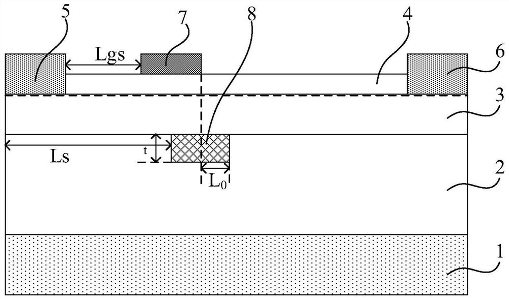
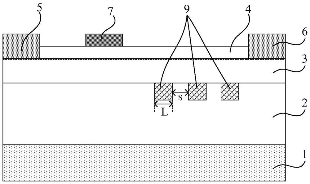
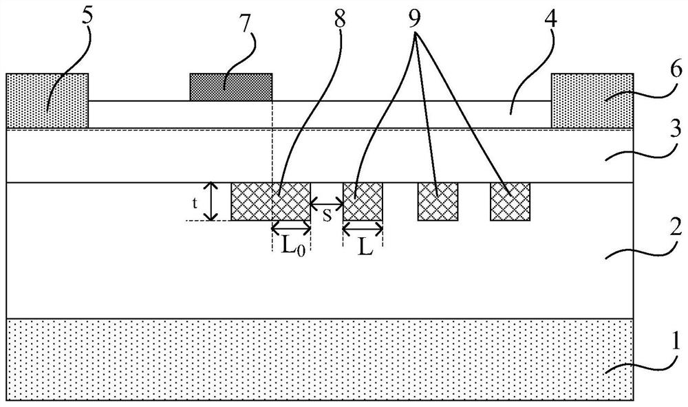
[0035] An embodiment of the present invention provides a semiconductor device, which is suitable for a device with high withstand voltage, and may include a heterojunction field effect transistor, such as a gallium nitride field effect transistor. The semiconductor device provided by the embodiment of the present invention includes: a substrate; a semiconductor layer located on the substrate; a source electrode, a drain electrode located on the side of the semiconductor ...


PUM

PropertyMeasurementUnit
lengthaaaaaaaaaa
lengthaaaaaaaaaa
thicknessaaaaaaaaaa

Abstract

The invention discloses a semiconductor device and a manufacturing method thereof. The semiconductor device comprises: a substrate; a semiconductor layer which is located on the substrate, wherein two-dimensional electron gas is formed in the semiconductor layer; and a source electrode and a drain electrode which are located on the side, away from the substrate, of the semiconductor layer, and a grid electrode which is located between the source electrode and the drain electrode, wherein a buried layer is formed in the semiconductor layer on one side, close to the substrate, of the two-dimensional electron gas, the buried layer and the semiconductor layer form a pn junction, the buried layer comprises a first buried layer and / or at least one second buried layer, the edge, close to the drain electrode, of the grid electrode is overlapped with the first buried layer, one part of the first buried layer extends from the edge, close to the drain electrode, of the grid electrode to the drainelectrode, and / or the second buried layer is located between the grid electrode and the drain electrode. According to the embodiment of the invention, the buried layer is formed in the semiconductorlayer, so that the breakdown voltage of the semiconductor device is improved.

Description

technical field [0001] Embodiments of the present invention relate to the technical field of semiconductors, and in particular, to a semiconductor device and a manufacturing method thereof. Background technique [0002] Gallium nitride, a semiconductor material, has become a research hotspot because of its wide band gap, high electron saturation drift velocity, high breakdown field strength and good thermal conductivity. In terms of electronic devices, gallium nitride materials are more suitable for manufacturing high-temperature, high-frequency, high-voltage and high-power devices than silicon and gallium arsenide, so gallium nitride-based electronic devices have good application prospects. [0003] In conventional gallium nitride field effect transistors, the electric field near the gate is densely distributed near the drain (called electric field concentration effect), which is easy to cause device breakdown; and electrons in the buffer layer will cause carrier collisions...

Claims


Application Information

Patent Timeline
Patent Type & Authority Applications(China)
IPC IPC(8): H01L29/778H01L29/06H01L21/335
CPCH01L29/7786H01L29/0623H01L29/66462
Inventor 裴晓延
Owner GPOWER SEMICON
Why Eureka
Try Eureka