Back metallized semiconductor structure and preparation method thereof
A technology of backside metallization and backside metallization, applied in semiconductor/solid-state device manufacturing, semiconductor devices, semiconductor/solid-state device components, etc., can solve problems such as bending and sagging, fragmentation, and wafer fragmentation, and reduce product production. cost, avoid the risk of fragmentation, and improve the effect of product yield
- Summary
- Abstract
- Description
- Claims
- Application Information
AI Technical Summary
Problems solved by technology
Method used
Image

Examples
Embodiment 1
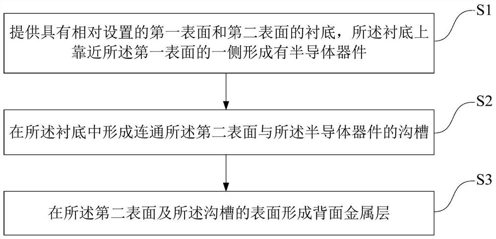
[0062] see Figure 1 to Figure 8 , the invention provides a method for preparing a backside metallized semiconductor structure, comprising the following steps:
[0063] 1) providing a substrate 101 having a first surface and a second surface oppositely arranged, and a semiconductor device 102 is formed on a side of the substrate 101 close to the first surface;
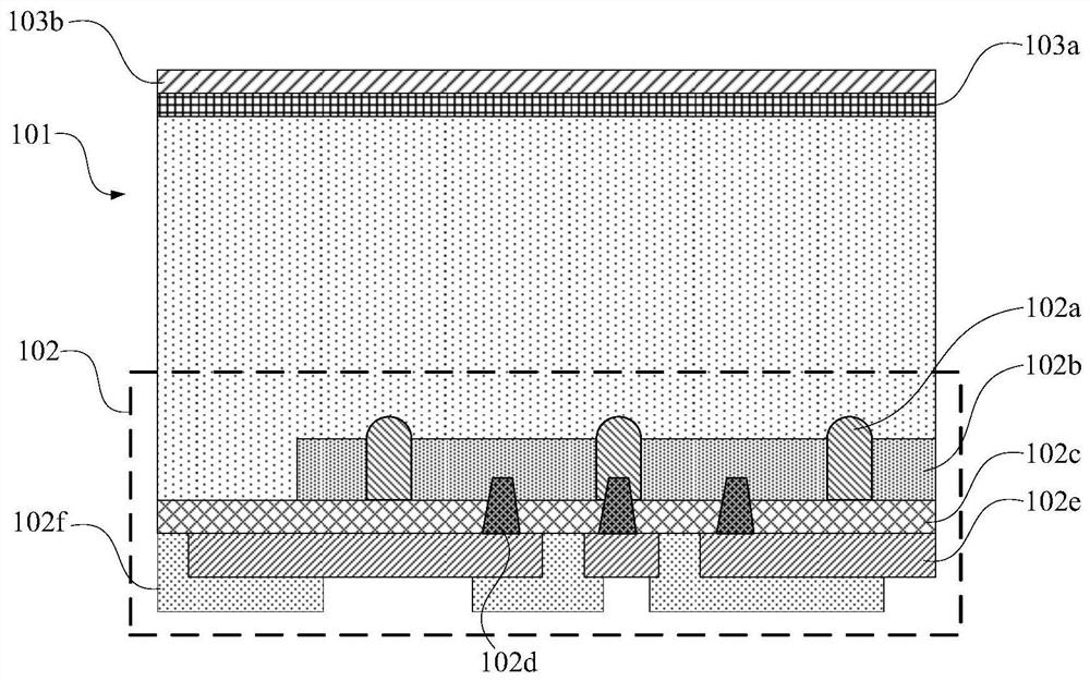
[0064] 2) forming a trench 103 connecting the second surface and the semiconductor device in the substrate 101;
[0065] 3) forming a back metal layer 104 on the second surface and the surface of the groove 103;
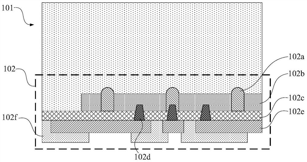
[0066] In step 1), see figure 1 The S1 step and figure 2 A substrate 101 having a first surface and a second surface opposite to each other is provided, and a semiconductor device 102 is formed on a side of the substrate 101 close to the first surface. exist figure 2Among them, the lower surface of the substrate 101 is the first surface, and the upper surface of the substrate 101 is the second surface....
Embodiment 2
[0087] Such as Figure 8 As shown, the present invention also provides a backside metallized semiconductor structure, comprising:
[0088] a substrate 101 having oppositely disposed first and second surfaces;
[0089] a semiconductor device 102, the semiconductor device 102 is formed on a side of the substrate 101 close to the first surface;
[0090] a trench 103, the trench 103 is formed in the substrate 101, and communicates with the second surface and the semiconductor device 102;
[0091] The back metal layer 104 is located on the second surface and the surface of the trench 103 .
[0092] As an example, the semiconductor device 102 includes a power MOS device. The semiconductor device 102 can be formed on the substrate 101 through an existing integrated circuit manufacturing process. Such as Figure 8 As shown, the power MOS device structure includes: a trench gate 102a, an implanted doped region 102b, a bottom dielectric layer 102c, a contact hole plug 102d, a metal...
Embodiment 3
[0096] This embodiment provides a backside metallized semiconductor structure. Compared with Embodiment 2, the difference of this embodiment is that a plurality of semiconductor devices and a plurality of trenches are formed in the substrate, and a plurality of trenches are formed in the substrate. The trenches are in one-to-one correspondence with a plurality of the semiconductor devices.
[0097] In the first embodiment, if Figure 8 As shown, one semiconductor device 102 and three trenches 103 are formed in the substrate 101 . However, in this embodiment, the plurality of trenches in the substrate correspond to a plurality of semiconductor devices one by one, that is, for a single semiconductor device on a wafer, only one trench passes through the plurality of semiconductor devices. The substrate reaches its backside. Specifically, the shape and size of the bottom surface of the groove is the same as that of the semiconductor device, that is, by setting the groove, the bo...
PUM
| Property | Measurement | Unit |
|---|---|---|
| thickness | aaaaa | aaaaa |
Abstract
Description
Claims
Application Information
 - Generate Ideas
- Intellectual Property
- Life Sciences
- Materials
- Tech Scout
- Unparalleled Data Quality
- Higher Quality Content
- 60% Fewer Hallucinations
Browse by: Latest US Patents, China's latest patents, Technical Efficacy Thesaurus, Application Domain, Technology Topic, Popular Technical Reports.
© 2025 PatSnap. All rights reserved.Legal|Privacy policy|Modern Slavery Act Transparency Statement|Sitemap|About US| Contact US: help@patsnap.com