A kind of heterogeneous semiconductor thin film and preparation method thereof

A semiconductor and thin film technology, applied in the field of heterogeneous semiconductor thin films and their preparation, can solve the problems of low ion utilization rate, prone to fragmentation, and high production cost, and achieves reduction of the risk of fragmentation, excellent material properties, and reduced implantation dose. Effect

Active Publication Date: 2021-12-28
SHANGHAI INST OF MICROSYSTEM & INFORMATION TECH CHINESE ACAD OF SCI
View PDF0 Cites 0 Cited by
  • Summary
  • Abstract
  • Description
  • Claims
  • Application Information

AI Technical Summary

Problems solved by technology

However, semiconductor thin films prepared based on ion stripping technology often have more defects, the utilization rate of stripped ions is not high, and the preparation cost is high.
In addition, thermal mismatch issues arise due to the lower limit of implant dose and energy required by this technology, resulting in a risk of fragmentation
To sum up: On the one hand, in the process of preparing semiconductor films based on ion stripping technology, the thermal mismatch between semiconductors and other substrates is relatively serious, and debris is prone to occur during annealing; on the other hand, the ion utilization rate required for stripping semiconductors is not high enough High, excess ions will aggravate the damage to the material

Method used


Image

  • A kind of heterogeneous semiconductor thin film and preparation method thereof
  • A kind of heterogeneous semiconductor thin film and preparation method thereof

Examples


preparation example Construction

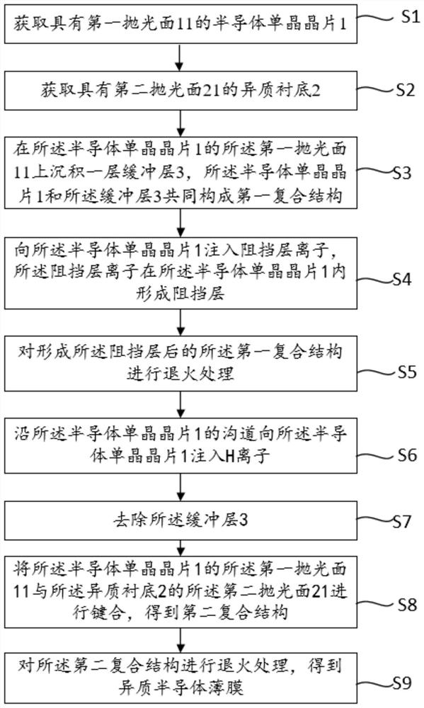
[0022] to combine figure 1 and figure 2 As shown, the implementation of the present invention provides a method for preparing a heterogeneous semiconductor thin film, the method comprising the following steps:

[0023] S1. Obtain a semiconductor single crystal wafer 1 having a first polished surface 11;

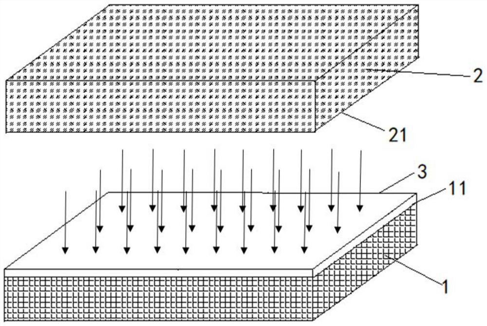
[0024] S2. Acquire a second polishing surface 21 ( figure 1 heterogeneous substrate 2 where the mid-bottom surface is not visible);

[0025] S3. Deposit a layer of buffer layer 3 on the first polished surface 11 of the semiconductor single crystal wafer 1, the semiconductor single crystal wafer 1 and the buffer layer 3 together form a first composite structure;

[0026] S4, implanting barrier layer ions into the semiconductor single crystal wafer 1, and the barrier layer ions form a barrier layer in the semiconductor single crystal wafer 1;

[0027] S5. Perform annealing treatment on the first composite structure after forming the barrier layer: the annealing temperature...

specific Embodiment approach 1

[0042] combined with figure 2 , the steps are as follows: obtain a lithium niobate single crystal wafer with the first polished surface, the size of the lithium niobate single crystal wafer is 4inch (inch), and the thickness is 500 μm (micrometer), and the surface roughness of the first polished surface is 0.5nm (nano); obtain a SiC substrate with a second polished surface, the size of the SiC substrate is 4inch, the thickness is 400 μm, and the surface roughness of the second polished surface is 0.3nm; in the first polishing of lithium niobate single crystal wafer Al on the surface is deposited with a thickness of 20nm by ALD (atomic layer deposition) 2 o 3 layer, LiNbO3 single crystal wafer and Al 2 o 3 The layers together form a first composite structure. Subsequently, the implantation energy to the lithium niobate single crystal wafer was 140Kev, and the implantation dose was 5*10 14 ions / cm 2 Ar ions, the implantation depth is 50nm from the outer surface of the buf...

specific Embodiment approach 2

[0043] combined with figure 2 , the steps are as follows: obtain a gallium nitride single crystal wafer with a first polished surface, the size of the gallium nitride single crystal wafer is 5 inches, the thickness is 460 μm, and the surface roughness of the first polished surface is 0.6 nm; obtain a gallium nitride single crystal wafer with a second polished surface Si substrate on the surface, the size of the Si substrate is 4inch, the thickness is 400μm, the surface roughness of the second polished surface is 0.3nm; ALD (atomic layer deposition) is used on the first polished surface of the gallium nitride single crystal wafer method to deposit HfO with a thickness of 20nm 2 layers, GaN monocrystalline wafers and HfO 2 The layers together form a first composite structure. Subsequently, the implantation energy to the gallium nitride single crystal wafer is 80Kev, and the implantation dose is 5*10 13 ions / cm 2 Ar ions, the implantation depth is 50nm from the outer surface...


PUM

PropertyMeasurementUnit
sizeaaaaaaaaaa
thicknessaaaaaaaaaa
surface roughnessaaaaaaaaaa

Abstract

The invention discloses a method for preparing a heterogeneous semiconductor thin film, comprising: obtaining a semiconductor single crystal wafer with a first polished surface; obtaining a heterogeneous substrate with a second polished surface; After depositing a layer of buffer layer on the top to form the first composite structure; implanting barrier layer ions into the semiconductor single crystal wafer to form a barrier layer; annealing treatment; implanting H ions into the semiconductor single crystal wafer along the channel of the semiconductor single crystal wafer, the H ion The atomic number is smaller than the atomic number of the barrier layer ions, and the implantation energy is greater than the implantation energy of the barrier layer ions; the buffer layer is removed; the semiconductor single crystal wafer is bonded to the heterogeneous substrate to obtain the second composite structure; annealing treatment is obtained to obtain the heterogeneous semiconductor film. The invention forms a barrier layer in the semiconductor single crystal wafer by implanting barrier layer ions to trap H ions, thus reducing damage caused by ion stripping, thereby greatly improving the utilization rate of H ions and the quality of the film.

Description

technical field [0001] The invention relates to the technical field of semiconductor materials, in particular to a heterogeneous semiconductor thin film and a preparation method thereof. Background technique [0002] At present, the ion stripping technology has become mature, and this technology is mainly used to produce silicon-on-insulator, and can be extended to various semiconductors through this technology. However, semiconductor thin films prepared based on ion stripping technology often have many defects, the utilization rate of stripped ions is not high, and the preparation cost is high. In addition, thermal mismatch issues arise due to the lower limit of implant dose and energy required by this technology, which leads to the risk of fragmentation. To sum up: On the one hand, in the process of preparing semiconductor films based on ion stripping technology, the thermal mismatch between semiconductors and other substrates is relatively serious, and debris is prone to...

Claims


Application Information

Patent Timeline
Patent Type & Authority Patents(China)
IPC IPC(8): H01L21/18H01L21/265H01L21/34H01L21/425H01L21/50
CPCH01L21/34H01L21/187H01L21/2654H01L21/425H01L24/83H01L2224/83048H01L2224/83051
Inventor 欧欣徐文慧游天桂沈正浩
Owner SHANGHAI INST OF MICROSYSTEM & INFORMATION TECH CHINESE ACAD OF SCI
Why Eureka
Try Eureka