Silicon-based gallium nitride microwave device and preparation method thereof
A technology of microwave devices and silicon-based nitrogen, which is applied in semiconductor/solid-state device manufacturing, semiconductor devices, electrical components, etc., can solve the problems that microwave devices cannot be produced on a large scale, and achieve improved turn-on voltage, suppression of leakage, and lower energy band poor effect
- Summary
- Abstract
- Description
- Claims
- Application Information
AI Technical Summary
Problems solved by technology
Method used
Image
Examples
Embodiment 1
[0052] This embodiment provides a method for preparing a silicon-based gallium nitride microwave device, and the specific steps are as follows:
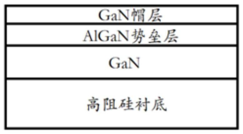
[0053] (1) The GaN-on-HRSi substrate is selected, and the substrate includes a high-resistance silicon-based substrate, a buffer layer (doped with C or Fe), a channel layer, a spacer layer, a barrier layer, and a cap layer from bottom to top. Organic cleaning, inorganic cleaning and other pretreatments are carried out on the substrate.
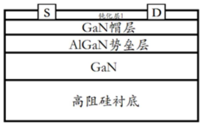
[0054] (2) Deposit about 50nm thick SiNx as a passivation layer on the substrate by LPCVD at 780°C; perform photolithography, development, and RIE etching on the device to expose the source and drain regions, and then perform ICP on the source and drain regions Etching, the conditions used for ICP etching are as follows: the atmosphere is Cl 2 / N 2 / O 2 : 40 / 10 / 5sccm, the chamber temperature is 20°C, the chamber pressure is 10mTorr, the ICP power is 150W, the RF power is 150W, the etching time is ...
Embodiment 2
[0061] The first passivation layer is made of LPCVDSiN in embodiment 1 step (2) x Replaced by PECVDSiO 2 , all the other are identical with embodiment 1, obtain silicon-based gallium nitride microwave device, the measured ohmic contact resistance ratio contact resistivity (same as embodiment 1 test conditions) is 5.57*10 -5 Ω*cm 2 , increased to 1.7 times of the original, and the ohmic contact metal edge is rough, and the phenomenon of diffusion to the surrounding is more obvious. Figure 9 The first passivation layer is PECVDSiO 2 (a) and LPCVDSiN x (b) And the microscopic image after mesa etching, it can be observed that the edge of the former is rougher and the metal diffusion phenomenon is more obvious.
Embodiment 3
[0063] Change the first layer of passivation layer and the second layer of passivation layer into etching the first layer of passivation layer, the second layer of passivation layer, cap layer, barrier layer in embodiment 1 step (4), and the rest All are the same as in Example 1, and the silicon-based gallium nitride microwave device is obtained. It is estimated that the threshold voltage of the device will be significantly shifted in the positive direction, and may even reach a positive value, which can improve the stability of the device and reduce the non-working state. power consumption.
PUM
| Property | Measurement | Unit |
|---|---|---|
| thickness | aaaaa | aaaaa |
| width | aaaaa | aaaaa |
Abstract
Description
Claims
Application Information
 - R&D Engineer
- R&D Manager
- IP Professional
- Industry Leading Data Capabilities
- Powerful AI technology
- Patent DNA Extraction
Browse by: Latest US Patents, China's latest patents, Technical Efficacy Thesaurus, Application Domain, Technology Topic, Popular Technical Reports.
© 2024 PatSnap. All rights reserved.Legal|Privacy policy|Modern Slavery Act Transparency Statement|Sitemap|About US| Contact US: help@patsnap.com


