Composite film packaging method of top-emitting OLED
A technology of composite film and packaging method, which is applied in the direction of organic semiconductor devices, electrical components, electric solid devices, etc., can solve the problems of reducing luminous efficiency, destroying organic molecules and polymer structures, affecting the yield of devices, etc.
- Summary
- Abstract
- Description
- Claims
- Application Information
AI Technical Summary
Problems solved by technology
Method used
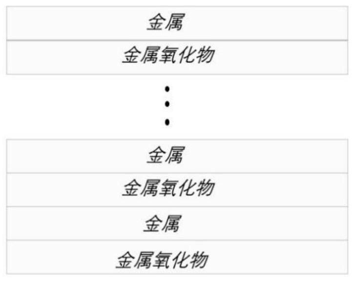
Image

Examples
Embodiment 1
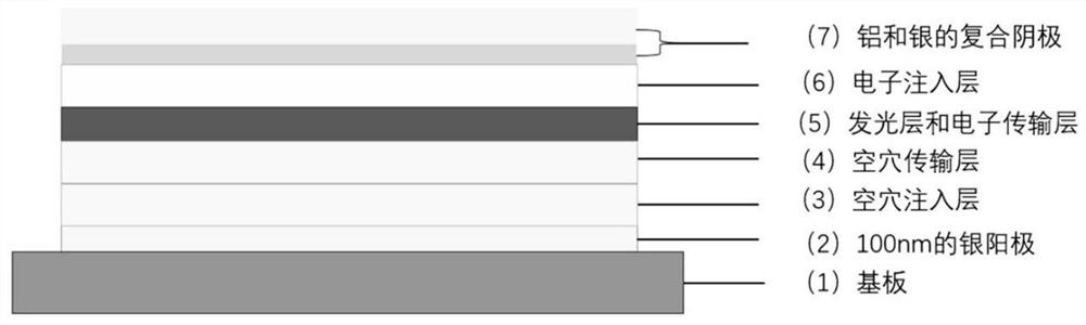
[0047] Step 1. Preparation of top-emitting OLED
[0048] 1. Cleaning the substrate: Put the ITO substrate into a glass tank filled with deionized water, add detergent powder and detergent, use an ultrasonic machine to ultrasonicate for 90 minutes, and then replace the solution in the tank with deionized water and acetone in turn , isopropanol, and ultrasonication for 90 minutes respectively to complete the cleaning of the substrate;
[0049] 2. Dry the substrate under the heating lamp, and UV treatment for 15 minutes, move the substrate into the vacuum evaporation cabin, and put the material to be evaporated on the substrate into the evaporation boat or crucible of the evaporation cabin, different evaporation sources The temperature can be controlled separately;
[0050] 3. Operate the instrument and evacuate the evaporation chamber to make the vacuum inside the evaporation chamber reach 10 -5 Below Pa, preheat the crucible so that the material to be evaporated reaches the e...
PUM
| Property | Measurement | Unit |
|---|---|---|
| Thickness | aaaaa | aaaaa |
| Thickness | aaaaa | aaaaa |
| Thickness | aaaaa | aaaaa |
Abstract
Description
Claims
Application Information
 - Generate Ideas
- Intellectual Property
- Life Sciences
- Materials
- Tech Scout
- Unparalleled Data Quality
- Higher Quality Content
- 60% Fewer Hallucinations
Browse by: Latest US Patents, China's latest patents, Technical Efficacy Thesaurus, Application Domain, Technology Topic, Popular Technical Reports.
© 2025 PatSnap. All rights reserved.Legal|Privacy policy|Modern Slavery Act Transparency Statement|Sitemap|About US| Contact US: help@patsnap.com