Solar energy selective absorber materials utilizing multiple photonic heterostructure interfaces
A technology of heterostructure and absorbing materials, applied in the field of solar selective absorbing materials, can solve the problems of low absorption efficiency, low photothermal conversion efficiency, poor high temperature resistance, etc., achieve simple structure, improve photothermal conversion efficiency and performance excellent effect
- Summary
- Abstract
- Description
- Claims
- Application Information
AI Technical Summary
Problems solved by technology
Method used
Image
Examples
Embodiment 1
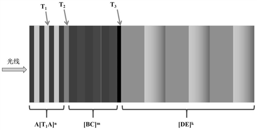
[0023] When n=2, m=3, k=4, the heterogeneous membrane structure is A[T 1 A] 2 T 2 [BC] 3 T 3 [DE] 4 .
[0024] Interference absorbing layer structure A[T 1 A] n Using multi-layer interference plays a major role in absorption. A dielectric film material is silicon nitride (Si 3 N 4 ), the refractive index n at the solar energy high-energy wavelength center at 550nm A is 2, then the thickness d A =550nm / 4nA ≈70nm; absorbing film layer T 1 It is metal titanium Ti, thickness d T1 10nm.
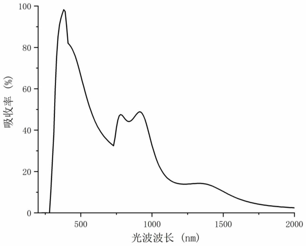
[0025] Visible light control film structure[BC] m The photon band gap effect is used to achieve high reflection and absorption in the 0.4-0.78 visible light absorption band. B dielectric film material is magnesium fluoride (MgF 2 ), the refractive index n B is 1.38; the C dielectric film material is titanium oxide (TiO 2 ), the refractive index n C is 2.6. There is a dimensional design relation for n B d B +n C d C =λ 1 / 2, λ 1 It takes a value in the range of 450-700nm, ...
Embodiment 2
[0030] When n=3, m=4, k=6, the heterogeneous membrane structure is A[T 1 A] 3 T 2 [BC] 4 T 3 [DE] 6 .
[0031] Interference absorbing layer structure A[T 1 A] n Using multi-layer interference plays a major role in absorption. A dielectric film material is titanium oxide (TiO 2 ), the refractive index n at the solar energy high-energy wavelength center at 550nm A is 2.6, then the thickness d A =550nm / 4n A ≈52nm; the absorption layer T1 is polysilicon (Si), the thickness d T1 10nm.
[0032] Visible light control film structure[BC] m The photon band gap effect is used to achieve high reflection and absorption in the 0.4-0.78 visible light absorption band. B dielectric film material is titanium oxide (TiO 2 ), the refractive index n C 2.6; C dielectric film material is silicon oxide (SiO 2 ), the refractive index n E is 1.46. There is a dimensional design relation for n B d B +n C d C =λ 1 / 2, take the value within the range of 450-700nm. Here, λ 1 The va...
PUM
| Property | Measurement | Unit |
|---|---|---|
| thickness | aaaaa | aaaaa |
| thickness | aaaaa | aaaaa |
| thickness | aaaaa | aaaaa |
Abstract
Description
Claims
Application Information
 - R&D
- Intellectual Property
- Life Sciences
- Materials
- Tech Scout
- Unparalleled Data Quality
- Higher Quality Content
- 60% Fewer Hallucinations
Browse by: Latest US Patents, China's latest patents, Technical Efficacy Thesaurus, Application Domain, Technology Topic, Popular Technical Reports.
© 2025 PatSnap. All rights reserved.Legal|Privacy policy|Modern Slavery Act Transparency Statement|Sitemap|About US| Contact US: help@patsnap.com


