
Processing method of sound hole of MEMS carrier plate

A processing method and sound hole technology, which is applied in the field of sound hole processing, can solve problems such as the deterioration of sound hole and graphic accuracy, affect the quality of sound holes, and waste costs, so as to improve processing accuracy, control the quality and roughness of sound holes controllable effect

Inactive Publication Date: 2020-08-14
JIANGSU PROVISION ELECTRONICS CO LTD
View PDF3 Cites 2 Cited by
  • Summary
  • Abstract
  • Description
  • Claims
  • Application Information

AI Technical Summary

Problems solved by technology

[0004] However, for the above-mentioned first processing technology, when the designed sound hole is located at the blind groove, then when performing laser grooving, because there are through holes (acoustic holes) in the area where the groove needs to be burnt, the energy will pass through the through hole and damage the Hole wall, which affects the quality of the sound hole
For the above-mentioned second processing technology, because the sound hole adopts two drilling operations, on the one hand, it will cause the accuracy of the sound hole and the graphics to deteriorate, and on the other hand, it will increase the process, resulting in cost waste

Method used


Image

  • Processing method of sound hole of MEMS carrier plate
  • Processing method of sound hole of MEMS carrier plate
  • Processing method of sound hole of MEMS carrier plate

Examples


Embodiment 1

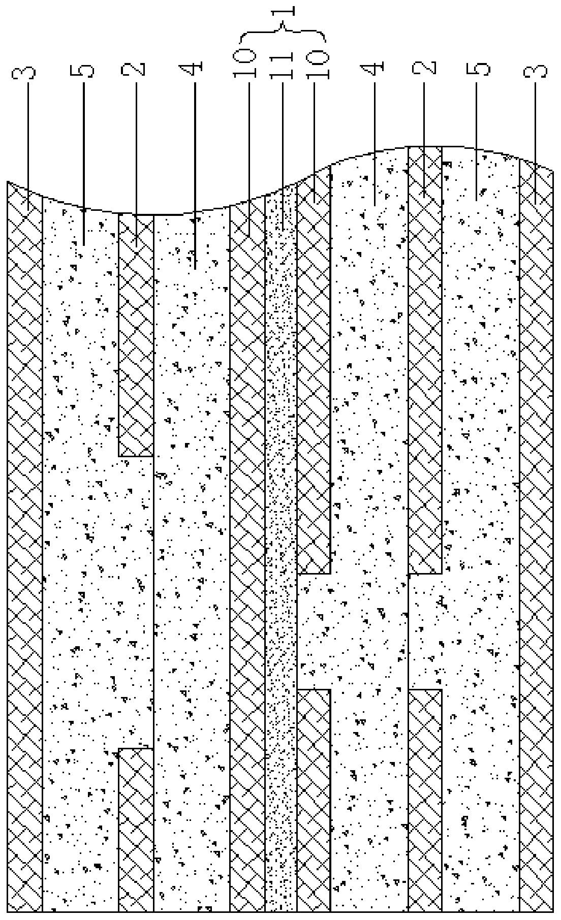
[0026] The invention provides a method for processing an acoustic hole of a MEMS carrier board, comprising the following steps: step 1), preparing a MEMS carrier board, for details, please refer to the attached figure 1 As shown, the MEMS carrier board includes a core board 1, two first copper layers 2 and two second copper layers 3, wherein the core board 1 is composed of two inner copper layers 10 through an inner insulating layer in the middle 11 by pressing and compounding, the two first copper layers 2 are respectively laminated on the surfaces of the two inner copper layers 10 through a first insulating layer 4, and the two second copper layers 3 are respectively Pressing on the two surfaces of the first copper layer 2 through a second insulating layer 5;

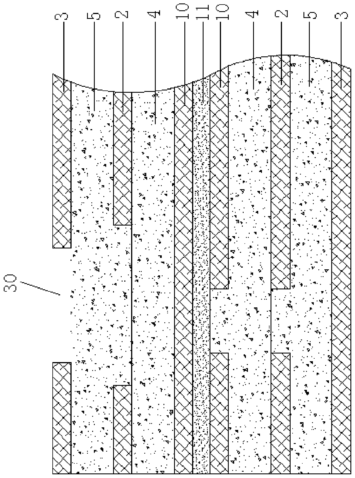
[0027] Step 2), according to the requirements of circuit layout, perform laser window opening operation on the second copper layer 3 to form a window 30 that can expose part of the surface of the second insulating lay...


PUM

PropertyMeasurementUnit
Groove depthaaaaaaaaaa
Groove widthaaaaaaaaaa
Slot lengthaaaaaaaaaa

Abstract

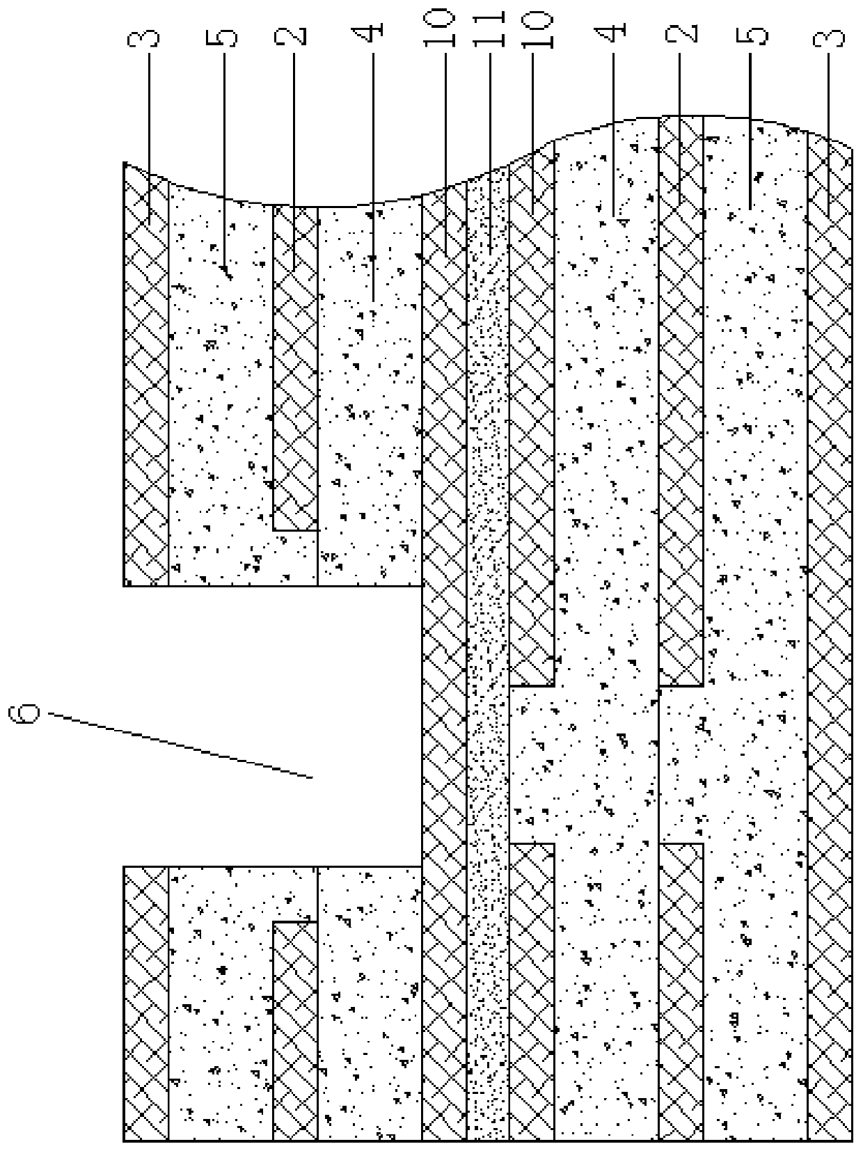
The invention discloses a processing method of a sound hole of an MEMS carrier plate. The method comprises the following steps: preparing an MEMS carrier plate, wherein the MEMS carrier plate comprises a core plate formed by laminating and compounding two inner copper layers and an inner insulating layer, two first copper layers laminated on the surfaces of the two inner copper layers through a first insulating layer respectively, and two second copper layers laminated on the surfaces of the two first copper layers through a second insulating layer respectively; performing laser windowing on the second copper layers to form a window capable of exposing a local surface of the second insulating layer; performing laser ablation grooving on the exposed surface area of each second insulating layer, and processing a blind groove capable of penetrating through the second insulating layer and the first insulating layer; and carrying out laser hole cutting on the MEMS carrier plate and at the position corresponding to the bottom of the blind groove, and processing a sound hole with one end communicated with the blind groove and the other end penetrating through the other second copper layer. The sound hole processing method has the advantages of being simple, easy to operate, high in operation precision, high in machining efficiency and the like, and the sound hole quality is guaranteed.

Description

technical field [0001] The invention relates to the technical field of circuit board production, and specifically provides a method for processing an acoustic hole of a MEMS carrier board. Background technique [0002] With the development of electronic technology and people's requirements for miniaturization and high integration of electronic products, in order to reduce the volume of the carrier board and increase the utilization rate of space, blind slot products have emerged as the times require. [0003] In the existing technology, the processing technology of blind groove and sound hole mainly adopts: the first processing technology: first perform mechanical drilling (sound hole) operation, then perform laser groove window opening operation, and then perform CO2 laser groove burning operation; or , the second processing technology: first carry out the laser groove window opening operation, then carry out the CO2 laser groove burning operation, and then carry out the X-...

Claims


Application Information

Patent Timeline
IPC IPC(8): H05K3/00B81C1/00
CPCH05K3/0026B81C1/00087B81C1/00547H05K2203/107
Inventor 马洪伟宗芯如杨飞
Owner JIANGSU PROVISION ELECTRONICS CO LTD
Learn More