A kind of semiconductor nanostructure photodetection device and its preparation method

A photodetector, nanostructure technology, applied in semiconductor devices, electrical components, circuits, etc., can solve the problems of slow response speed of semiconductor nanostructures, mismatch of resonance wavelength and detection wavelength, etc., to achieve high sensitivity, enhanced light absorption, The effect of high quantum efficiency

Active Publication Date: 2021-12-10
SUN YAT SEN UNIV
View PDF0 Cites 1 Cited by
  • Summary
  • Abstract
  • Description
  • Claims
  • Application Information

AI Technical Summary

Problems solved by technology

[0006] The present invention provides a semiconductor nanostructure in order to overcome the problem of the mismatch between the resonance wavelength and the detection wavelength when the same structure is used to simultaneously realize the resonance and photosensitive functions in the above-mentioned prior art, and the defect that the response speed of the semiconductor nanostructure modified by precious metal particles is slow photodetection device

Method used


Image

  • A kind of semiconductor nanostructure photodetection device and its preparation method
  • A kind of semiconductor nanostructure photodetection device and its preparation method
  • A kind of semiconductor nanostructure photodetection device and its preparation method

Examples


Embodiment 1

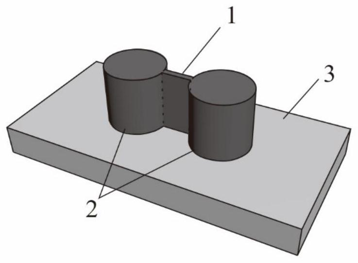
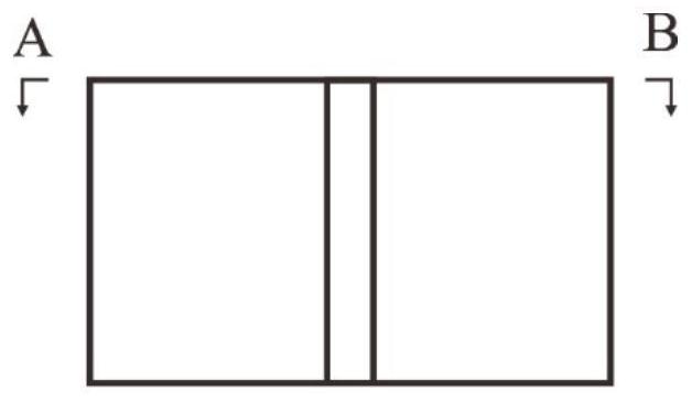
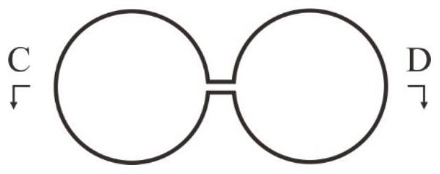
[0044] A semiconductor nanostructure photodetection device, such as Figure 1~3 As shown, it is composed of a nanochannel 1 in the middle and antenna units 2 at both ends, and is a dumbbell-shaped integrated structure.

[0045] In this embodiment, the shape of the antenna unit is a cylinder. Semiconductor nanostructured photodetection devices are made of silicon.

[0046] The diameter, height or edge of the antenna unit can be 50-500nm, such as 50nm, 120nm, 150nm, 200nm, 400nm or 500nm. In this embodiment, the height of the antenna unit is 150nm, and the diameter is 120nm.

[0047] The length of the nano-channel may be 10-100 nm, such as 5 nm, 10 nm, 20 nm, 50 nm, 100 nm or 200 nm. In this embodiment, the length of the nano-channel is 20 nm.

[0048] The width of the narrowest part of the nanochannel can be 5-30 nm, such as 5 nm, 10 nm, 20 nm or 30 nm. In this embodiment, the width of the narrowest part of the nanochannel is 10 nm.

[0049] The preparation method of the sem...

Embodiment 2

[0060] The difference from Example 1 is that the semiconductor nanostructure photodetection device of this example is made of germanium, boron, lead telluride, gallium arsenide, aluminum gallium arsenide, indium arsenide, gallium phosphide, gallium indium phosphide, phosphorus indium, gallium telluride, aluminum telluride or aluminum gallium telluride;

[0061] Other structures and materials are the same as in Example 1.

Embodiment 3

[0063] The difference from Embodiment 1 is that in the semiconductor nanostructure photodetection electrical device of this embodiment, the shape of the antenna element is a prism, a sphere or an ellipsoid;

[0064] Other structures and materials are the same as in Example 1.


PUM

PropertyMeasurementUnit
lengthaaaaaaaaaa
diameteraaaaaaaaaa
lengthaaaaaaaaaa

Abstract

The invention discloses a semiconductor nanostructure photodetection device and a preparation method thereof; the photodetector is a dumbbell-shaped integrated structure consisting of a nanochannel in the middle and antenna units capable of Mie resonance at both ends; The length of the nano-channel is 10-100nm, and the width of the narrowest part of the nano-channel is 5-30nm. When the photodetector works, the nanochannel is a photosensitive structure, and the antenna unit is a resonant structure. The detection light excites the Mie resonance of the antenna unit, and the light is localized to the interior of the nanochannel to enhance light absorption, generate photocurrent, and realize photodetection. The semiconductor nanostructure photodetection device of the present invention is integrated with a resonant structure and a photosensitive structure, which can enhance the light absorption of the semiconductor nanochannel, thereby realizing photodetection with high quantum efficiency, fast response, and high sensitivity, and can be used in image sensing and on-chip communication applications in other fields.

Description

technical field [0001] The invention relates to the technical field of semiconductor devices, and more specifically, to a semiconductor nanostructure photodetection device and a preparation method thereof. Background technique [0002] Semiconductor nanostructures have large specific surface areas and small sizes. Photodetectors based on semiconductor nanostructures usually have high sensitivity and high integration, and have promising applications in the fields of image sensing and on-chip communication. However, since the size of semiconductor nanostructures is usually smaller than the wavelength of the detected light, the semiconductor nanostructures can only absorb a small part of the detected light, resulting in low quantum efficiency and responsivity of photoelectric conversion. [0003] Enhancing the light absorption of semiconductor nanostructures is one of the main technical methods to improve the photodetection responsivity and quantum efficiency of semiconductor ...

Claims


Application Information

Patent Timeline
Patent Type & Authority Patents(China)
IPC IPC(8): H01L31/0232H01L31/0352H01L31/09H01L31/18
CPCH01L31/02327H01L31/0352H01L31/09H01L31/18Y02P70/50
Inventor 佘峻聪虞佳杰黄一峰邓少芝许宁生陈军
Owner SUN YAT SEN UNIV
Why Eureka
Try Eureka