
Laser annealing equipment

A technology of laser annealing and equipment, applied in the manufacturing of electrical components, electric solid-state devices, semiconductor/solid-state devices, etc., can solve the problems of poor contamination, affecting product yield, abnormal crystallization, etc.

Active Publication Date: 2020-07-24
BOE TECH GRP CO LTD +1
View PDF6 Cites 0 Cited by
  • Summary
  • Abstract
  • Description
  • Claims
  • Application Information

AI Technical Summary

Problems solved by technology

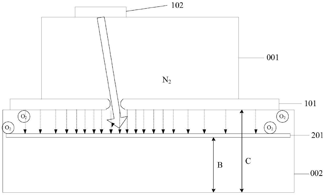
However, this method is likely to cause the nitrogen atmosphere at the laser exit slit to be unstable, which is specifically manifested in the high local oxygen concentration resulting in poor nitrogen flow disturbance (N 2 Turbulence Mura) phenomenon, resulting in the conversion of amorphous silicon to polysilicon (p-Si), the region with high oxygen concentration shows abnormal crystallization, and the roughness of the polysilicon film is too large, which can easily lead to the back-end gate (Gate) layer A short circuit (short) occurs with the channel film layer composed of polysilicon, which seriously affects the electrical properties of the transistor (TFT), and eventually causes the entire surface of the back-end (ET) to be dirty after lighting, which affects the product yield.

Method used


Image

  • Laser annealing equipment
  • Laser annealing equipment
  • Laser annealing equipment

Examples


Embodiment Construction

[0032] In order to make the purpose, technical solutions and advantages of the embodiments of the present invention more clear, the following will clearly and completely describe the technical solutions of the embodiments of the present invention in conjunction with the drawings of the embodiments of the present invention. Apparently, the described embodiments are some, not all, embodiments of the present invention. Based on the described embodiments of the present invention, all other embodiments obtained by persons of ordinary skill in the art without creative efforts shall fall within the protection scope of the present invention.

[0033] Unless otherwise defined, the technical terms or scientific terms used herein shall have the usual meanings understood by those skilled in the art to which the present invention belongs. "First", "second" and similar words used in the description and claims of the present invention do not indicate any order, quantity or importance, but ar...


PUM


Abstract

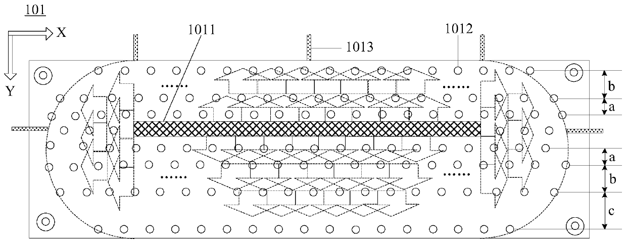
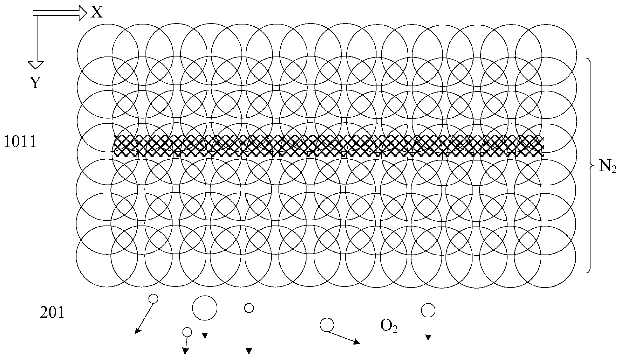
The invention discloses laser annealing equipment which comprises a deoxidation chamber, an excimer laser generator located above the deoxidation chamber and an annealing chamber located below the deoxidation chamber. The annealing chamber comprises a bearing table used for bearing a substrate with an amorphous silicon film; the deoxidation chamber comprises a bottom cover plate, an annealing window and a nitrogen conveying pipe; the bottom cover plate comprises a laser exit slit and a plurality of gas diffusion holes distributed around the laser exit slit; nitrogen provided by the nitrogen conveying pipe fills the deoxidation chamber and diffuses to the bearing table through the laser exit slit and the gas diffusion holes; and a laser emitted by the excimer laser generator is emitted to the bearing table through the annealing window and the laser exit slit in sequence. The multiple gas diffusion holes are additionally formed in a periphery of the laser exit slit so that a nitrogen atmosphere blown to the surface of the bearing table by the laser exit slit and the gas diffusion holes is uniform, a melting recrystallization area is in a pure nitrogen environment, crystallization quality is improved, and then a product yield is increased.

Description

technical field [0001] The invention relates to the technical field of display preparation, in particular to a laser annealing device. Background technique [0002] In flat panel display devices, Active Matrix Organic Light Emitting Diode (AMOLED) has become the future due to its advantages of high image quality, short response time of moving images, low power consumption, wide viewing angle and ultra-light and ultra-thin. The best choice for display technology. At present, in AMOLED, the polysilicon layer is produced in the backplane technology, including various production methods such as excimer laser annealing (ELA for short), solid phase crystallization or metal induced crystallization. However, using the excimer laser annealing process to obtain the polysilicon thin film of the active layer of the transistor in the backplane is the only method that has achieved mass production. [0003] The excimer laser annealing process is a relatively complicated annealing process...

Claims


Application Information

Patent Timeline
Patent Type & Authority Applications(China)
IPC IPC(8): H01L21/67H01L21/77H01L27/12H01L27/32
CPCH01L21/67115H01L21/77H01L27/1285H01L2021/775H10K59/12Y02P70/50
Inventor 汪庆路兆里刘松林全祥皓赵东升
Owner BOE TECH GRP CO LTD
Learn More