Metallized isolated scintillation ceramic array structure and preparation method thereof
A technology of scintillation ceramics and array structure, used in manufacturing tools, stone processing equipment, stone processing tools, etc., can solve the problems affecting detector clarity, radiation intensity crosstalk, array element information distortion, etc., and achieve strong X-ray absorption and Isolation capability, improved signal-to-noise ratio and resolution, effect of eliminating scattered line artifacts
- Summary
- Abstract
- Description
- Claims
- Application Information
AI Technical Summary
Problems solved by technology
Method used
Image
Examples
Embodiment 1
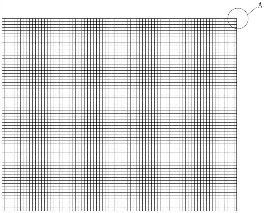
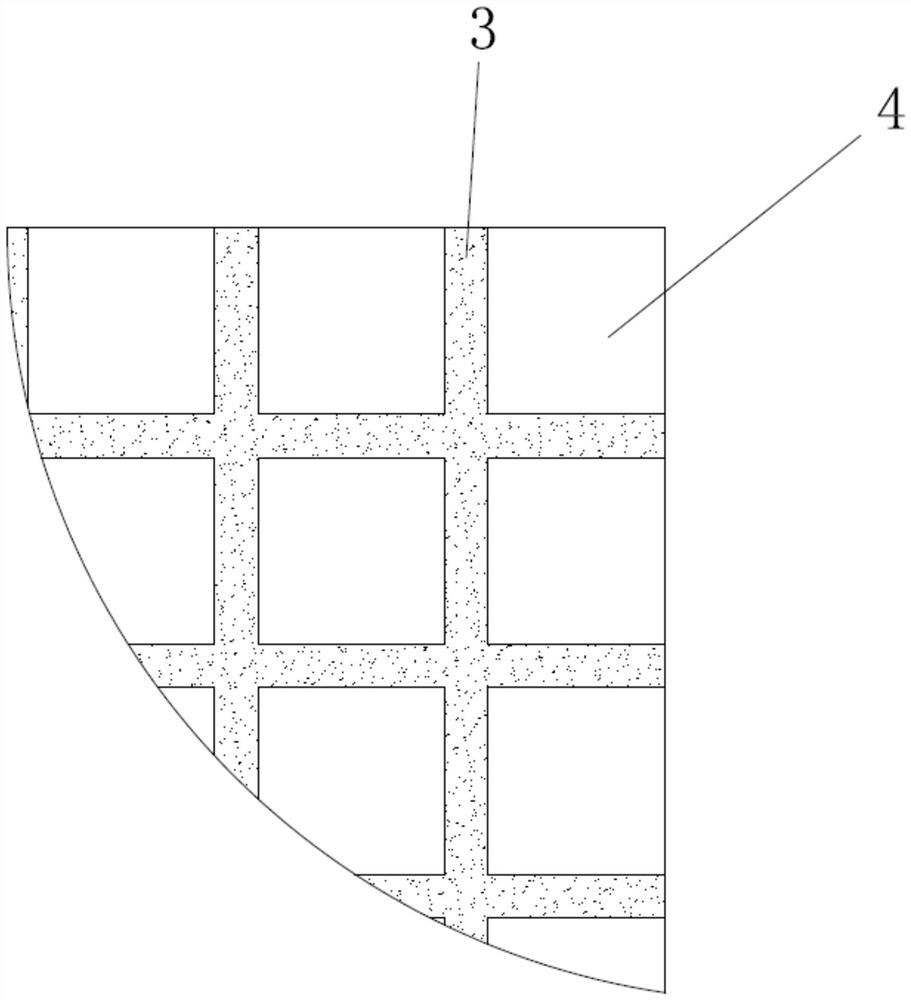
[0036] Such as Figure 1~4 The metallized and isolated scintillation ceramic array structure in this embodiment includes a scintillation ceramic block 1, on which scintillating ceramic block 1 is provided with criss-cross and interconnected slits 2, and both ends of the slits 2 communicate with the peripheral surface of scintillation ceramic block 1 The upper surface of the scintillation ceramic block 1 is divided into a plurality of scintillation ceramic array elements 4 distributed in a square array with the same size by the slot 2, and each slot 2 is filled with high-density sintered metal for isolating each scintillation ceramic array element Metallized isolation layer 3, the high-density sintered metallized isolation layer in this example is formed by sintering silver paste, and the silver paste is prepared according to the commonly used conductive silver paste for filters. The high-density sintered metal material can reduce the scattering of X-rays and secondary fluoresc...
Embodiment 2
[0051] The steps for preparing the scintillation ceramic array structure in this example are as follows:
[0052] Step 1: prepare scintillation ceramic powder slurry according to the ratio in the prior art, pour the scintillation ceramic powder slurry into a mold to make a raw scintillation ceramic blank; The sintering temperature is 1700°C, and the heat preservation is 9 hours. After a high-temperature sintering, it is cooled to form a flashing ceramic block;
[0053] Step 2: Fix the scintillation ceramic block on the substrate with glue, and use a diamond cutting knife to cut a plurality of criss-cross and interconnected grooves on the upper surface of the scintillation ceramic block. The depth of the cut grooves is the same as the total thickness of the scintillation ceramic block, that is Completely cut through the scintillation ceramic block, the width of the slit is 200 μm, the two ends of the slit are connected to the peripheral surface of the scintillation ceramic bloc...
PUM
| Property | Measurement | Unit |
|---|---|---|
| size | aaaaa | aaaaa |
Abstract
Description
Claims
Application Information
 - R&D
- Intellectual Property
- Life Sciences
- Materials
- Tech Scout
- Unparalleled Data Quality
- Higher Quality Content
- 60% Fewer Hallucinations
Browse by: Latest US Patents, China's latest patents, Technical Efficacy Thesaurus, Application Domain, Technology Topic, Popular Technical Reports.
© 2025 PatSnap. All rights reserved.Legal|Privacy policy|Modern Slavery Act Transparency Statement|Sitemap|About US| Contact US: help@patsnap.com


