Semiconductor device and manufacturing method thereof

A manufacturing method and semiconductor technology, applied in the fields of semiconductor/solid-state device manufacturing, semiconductor devices, electric solid-state devices, etc., can solve the problems of improvement, inability to perform electrical connection, and inability to optimize the electrical performance of back-illuminated CMOS image sensors. Performance optimization, electrical performance improvement, effect of electrical performance optimization

Active Publication Date: 2022-06-28
WUHAN XINXIN SEMICON MFG CO LTD
View PDF3 Cites 0 Cited by
  • Summary
  • Abstract
  • Description
  • Claims
  • Application Information

AI Technical Summary

Problems solved by technology

[0003] However, in the existing process of making a back-illuminated CMOS image sensor, there is a buffer medium layer between the metal grid in the pixel area and the underlying substrate and deep trench filling structure, so that the metal grid and the underlying There is only a physical connection between the substrate and the deep trench filling structure, but no electrical connection, which makes it impossible to optimize and improve the electrical performance of the back-illuminated CMOS image sensor

Method used


Image

  • Semiconductor device and manufacturing method thereof
  • Semiconductor device and manufacturing method thereof
  • Semiconductor device and manufacturing method thereof

Examples


Embodiment Construction

[0059] A fabrication process of a metal grid layer in a pixel area is as follows:

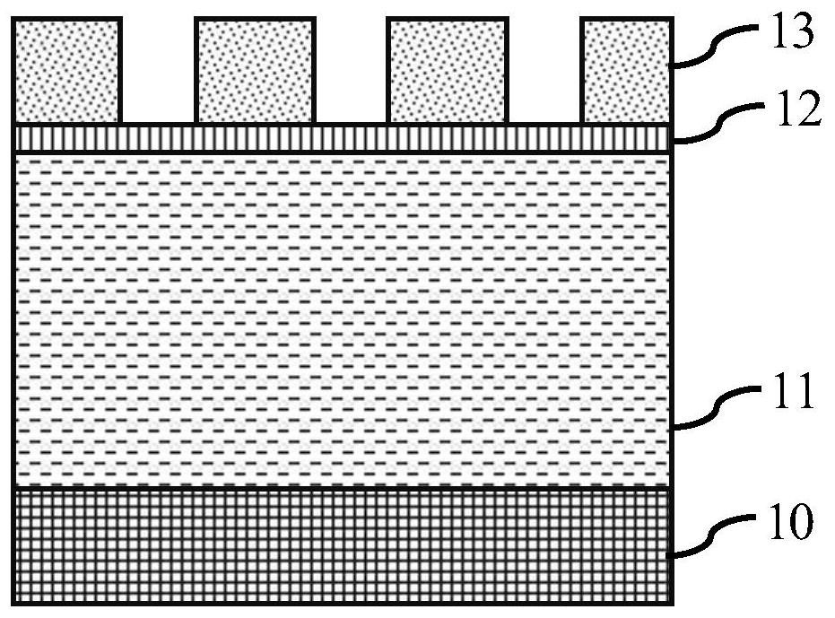
[0060] like Figure 1a As shown, a substrate 10 having a pixel region 11 is provided;

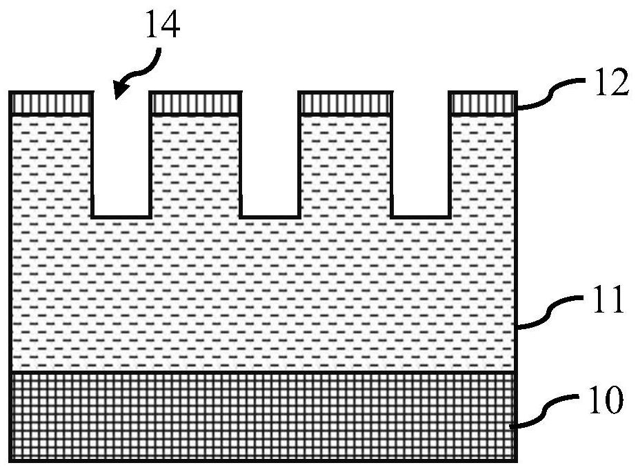
[0061] like Figure 1a and 1b As shown, a pad oxide layer 12 is formed on the pixel region 11 , a first patterned photoresist layer 13 is formed on the pad oxide layer 12 , and the first patterned photoresist layer 13 is formed on the pad oxide layer 12 . As a mask, the pad oxide layer 12 on the pixel area 11 and the substrate 10 with a partial thickness are etched to form trenches 14 in the substrate 10 of the pixel area 11, and the a patterned photoresist layer 13;

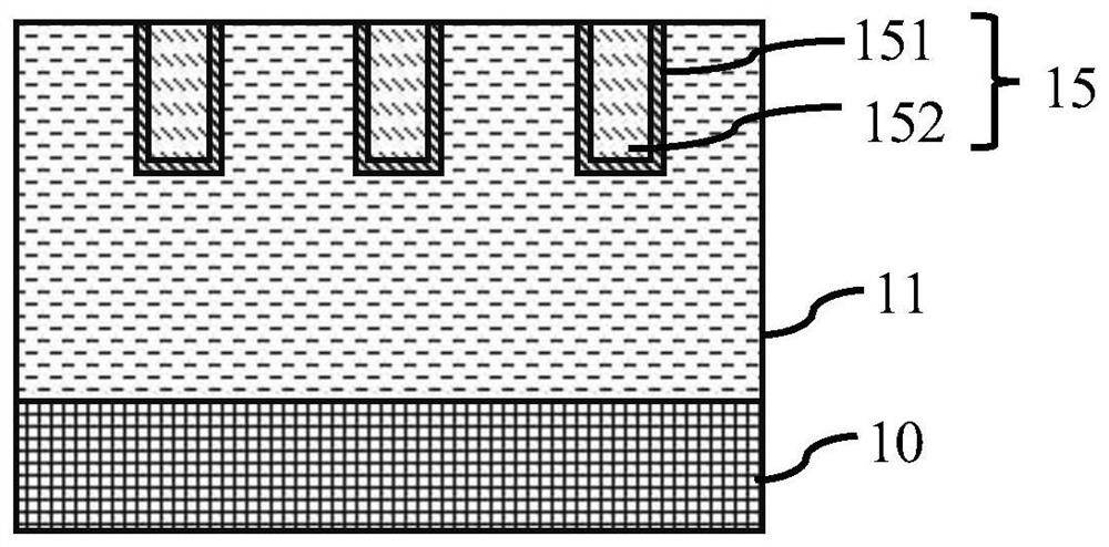
[0062] like Figure 1c As shown, an isolation oxide layer 151 is formed on the surface of the trench 14 and the surface of the pad oxide layer 12, and a conductive metal layer 152 is filled in the trench 14, and the conductive metal layer 152 covers all the On the pad oxide layer 12 , the conductive metal layer 152 , the isolation oxide ...


PUM


Abstract

The invention provides a semiconductor device and a manufacturing method thereof. The manufacturing method of the semiconductor device includes: forming a trench filling structure in the substrate of the pixel region, and the sidewall of the filling material in the trench filling structure and the substrate A high-K dielectric layer is also sandwiched between them; a plug structure is formed in the substrate of the pad area; the buffer dielectric layer is covered on the substrate surface of the pixel area and the pad area; the buffer dielectric layer is etched to form at least the exposed Part of the substrate at the periphery of the top sidewall of the trench-filling structure and / or a first opening at least part of the top of the trench-filling structure; and, forming a metal grid layer on the buffer medium layer of the pixel region and filling the first opening , so as to be electrically connected to the exposed part of the substrate and / or the trench filling structure. The technical solution of the present invention enables the metal grid layer to be electrically connected to the exposed part of the substrate and / or the trench filling structure, thereby enabling the optimization and improvement of the electrical performance of the semiconductor device.

Description

technical field [0001] The invention relates to the field of semiconductor integrated circuit manufacturing, in particular to a semiconductor device and a manufacturing method thereof. Background technique [0002] In the manufacturing process of Back-side Illumination CMOS Imagination Sensor (BSI-CIS), deep trench isolation (Deep Trench Isolation, DTI) technology and Backside Metal Grid (BMG for short) ) technology can make the back-illuminated CMOS image sensor have better optical performance. [0003] However, in the existing process of fabricating a back-illuminated CMOS image sensor, there is a buffer medium layer between the fabricated metal grid in the pixel region and the underlying substrate and the deep trench filling structure, so that the metal grid is connected to the underlying substrate and the deep trench filling structure. The substrate and the deep trench filling structure are only physically connected, and cannot be electrically connected, so that it is i...

Claims


Application Information

Patent Timeline
Patent Type & Authority Patents(China)
IPC IPC(8): H01L21/762H01L29/06
CPCH01L21/76224H01L29/0634H01L27/1463H01L27/14636H01L27/14683
Inventor 胡胜杨帆
Owner WUHAN XINXIN SEMICON MFG CO LTD
Why Eureka
Try Eureka