Display panel and preparation method thereof

A technology for display panels and substrates, used in static indicators, instruments, electrical components, etc., can solve the problem of inability to guarantee the high-quality display quality of display panels, and achieve the effects of avoiding poor display, accurate control, and reducing dependence.

Inactive Publication Date: 2020-05-29
WUHAN CHINA STAR OPTOELECTRONICS TECH CO LTD
View PDF4 Cites 3 Cited by
  • Summary
  • Abstract
  • Description
  • Claims
  • Application Information

AI Technical Summary

Problems solved by technology

[0003] In order to solve the above problems, the present invention provides a display panel and its preparation method to solve the technical problem in the prior art that the high-quality display quality of the display panel cannot be guaranteed while realizing a single control LED chip

Method used


Image

  • Display panel and preparation method thereof
  • Display panel and preparation method thereof
  • Display panel and preparation method thereof

Examples


Embodiment

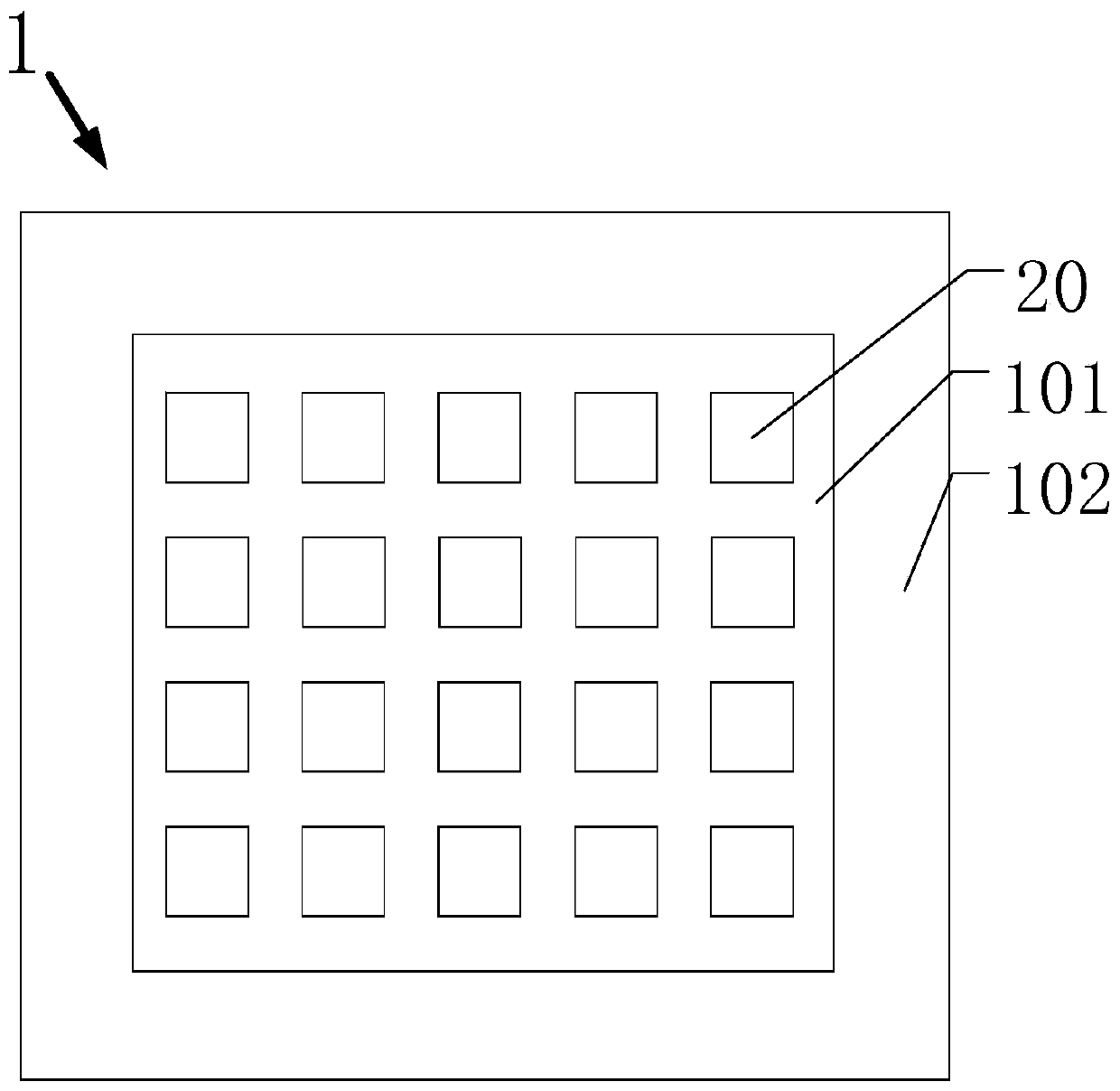
[0040] Such as figure 1 with Figure 8 As shown, in this embodiment, the display panel 1 of the present invention includes a first substrate 10 , LED chips 20 , a protective layer 30 and a reflective layer 40 .

[0041] The display panel 1 further includes a light emitting area 101 and a non-light emitting area 102 surrounding the light emitting area 101;

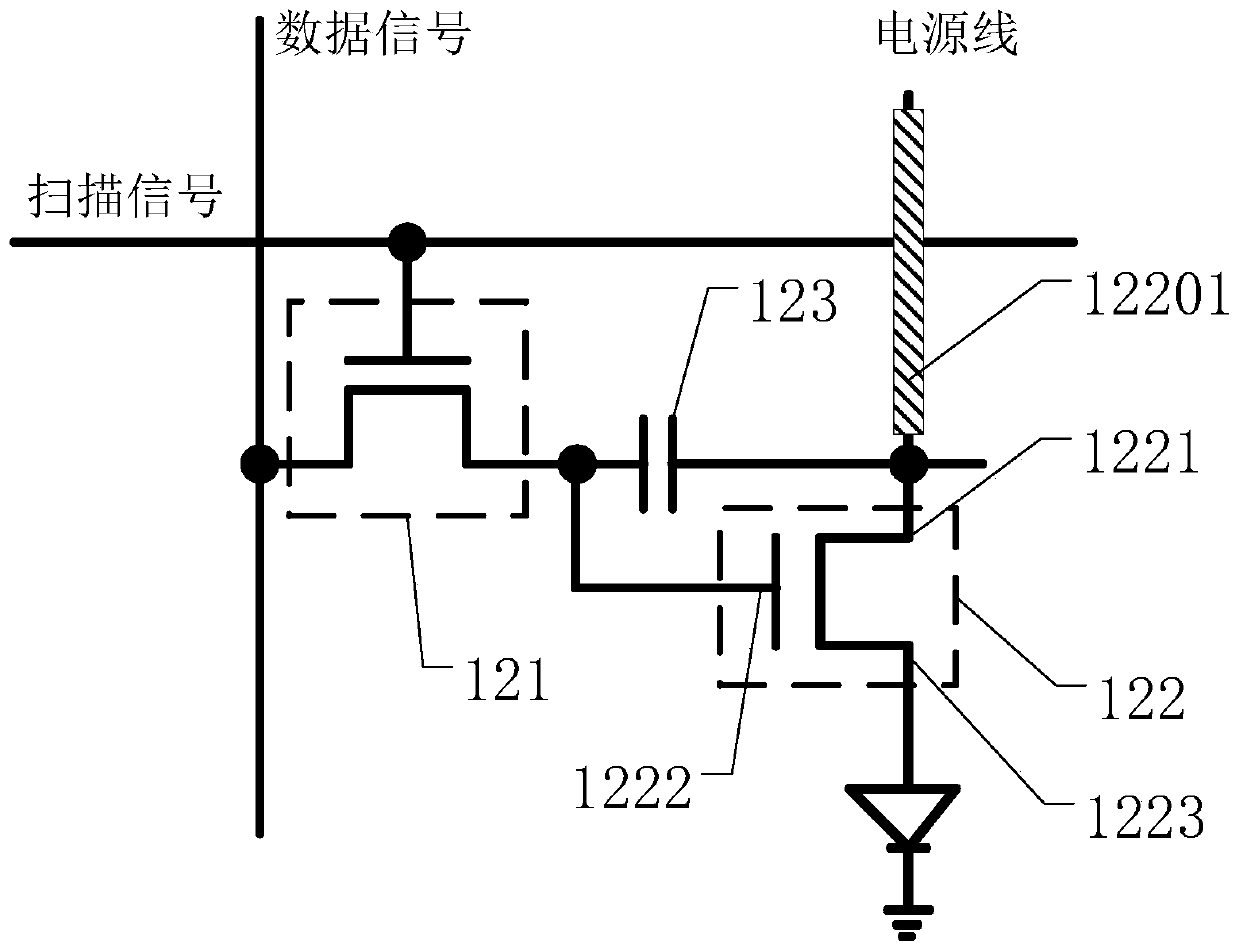
[0042] Such as Figure 5 As shown, the first substrate 10 includes a substrate 110 , a thin film transistor unit 120 , a data line 130 , a power line 140 and a GOA circuit 150 .

[0043] The LED chips 20 on the display panel 1 are individually controlled by the corresponding thin film transistor unit 120, so that the display panel 1 can realize partitioned display, thereby making the display picture more delicate and improving the display quality.

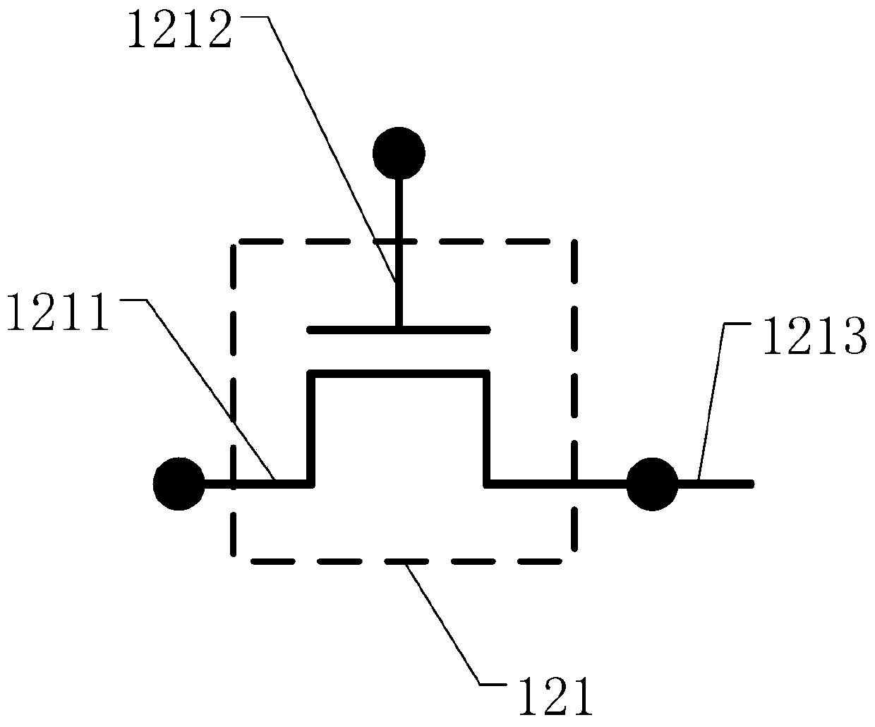
[0044] Such as figure 2 with image 3 As shown, specifically, a plurality of thin film transistor units 120 are arranged on the first substrate 10, and each thin film tran...


PUM


Abstract

The invention provides a display panel and a preparation method thereof. The display panel comprises a first substrate and a plurality of LED chips; the first substrate is provided with a plurality ofthin film transistor units; the plurality of LED chips are distributed on the first substrate in an array; each thin film transistor unit is correspondingly connected with and controls one LED chip.According to the display panel and the preparation method thereof, the array circuit is prepared on the glass substrate, so that each LED chip can be independently controlled; such kind of control mode can adjust and control display image quality more accurately, and an image quality improvement effect is more obvious. According to a gray scale driving mode, field frequency modulation driving is adopted, sequential control is simpler, dependence on liquid crystal response speed is reduced, and color cast caused by direct current driving is avoided. In the manufacturing process of the display substrate, voltage drop caused by circuit impedance is reduced by adding a high-conductivity metal wire on a power line, so that poor display is avoided. A nano-silver paste technology is adopted to solve the problem of chip bonding caused by a non-copper manufacturing process, and the manufacturing yield of the display panel is improved.

Description

technical field [0001] The present application relates to the display field, in particular to a display panel and a preparation method thereof. Background technique [0002] Mini-LED has many advantages such as high brightness, high contrast, low power consumption, special-shaped display, etc., and has recently been closely watched by the market. The development of Mini-LED in terms of structure and process is also becoming more and more mature. At present, the common mini-LED architecture is the COB or CSP assembly process of FPC / PCB substrates. Driver IC is used for PM drive, and the partition algorithm is used to realize HDR display. However, for the PM drive method, if the mini-LED panel has a large number of partitions and the size is small, the layout tends to generate more traces and cause the boundary to be too large. At the same time, the PM drive method is limited by the partition channels of the driver. , it is impossible to design more partitions, and the HDR di...

Claims


Application Information

Patent Timeline
Patent Type & Authority Applications(China)
IPC IPC(8): H01L25/16H01L27/15G09F9/33G09G3/32
CPCG09F9/33G09G3/32H01L25/167H01L27/156
Inventor 杨勇
Owner WUHAN CHINA STAR OPTOELECTRONICS TECH CO LTD
Why Eureka
Try Eureka