Three-dimensional memory and its preparation method

A memory, three-dimensional technology, applied in the direction of semiconductor devices, electrical solid devices, electrical components, etc., can solve the problems of serious inclination of the upper layer channel holes, affecting the electrical performance of the three-dimensional memory, and the inability to align the lower layer channel holes, etc., to achieve reduction Less risk of tilting, avoiding side wall damage, improving the effect of contour distortion

Active Publication Date: 2021-09-28
YANGTZE MEMORY TECH CO LTD
View PDF9 Cites 0 Cited by
  • Summary
  • Abstract
  • Description
  • Claims
  • Application Information

AI Technical Summary

Problems solved by technology

[0003] In view of this, the present application provides a three-dimensional memory and its preparation method to solve the problem that in the prior art, due to the increase in the number of stacked layers, the inclination of the channel holes in the upper layer becomes more and more serious, resulting in the inability to align with the channel holes in the lower layer. , and then when the bottom of the channel hole is etched later, it will cause sidewall damage and affect the electrical performance of the three-dimensional memory.

Method used


Image

  • Three-dimensional memory and its preparation method
  • Three-dimensional memory and its preparation method
  • Three-dimensional memory and its preparation method

Examples


Embodiment Construction

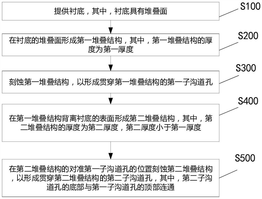
[0039] Specific embodiments of the present invention will be described in more detail below with reference to the accompanying drawings. Although exemplary embodiments of the invention are shown in the drawings, it should be understood that the invention may be practiced in other ways than those described herein, and therefore, the invention is not limited by the following embodiments.

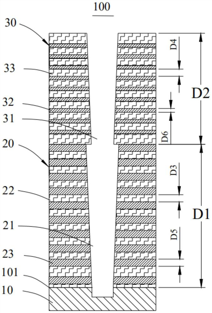
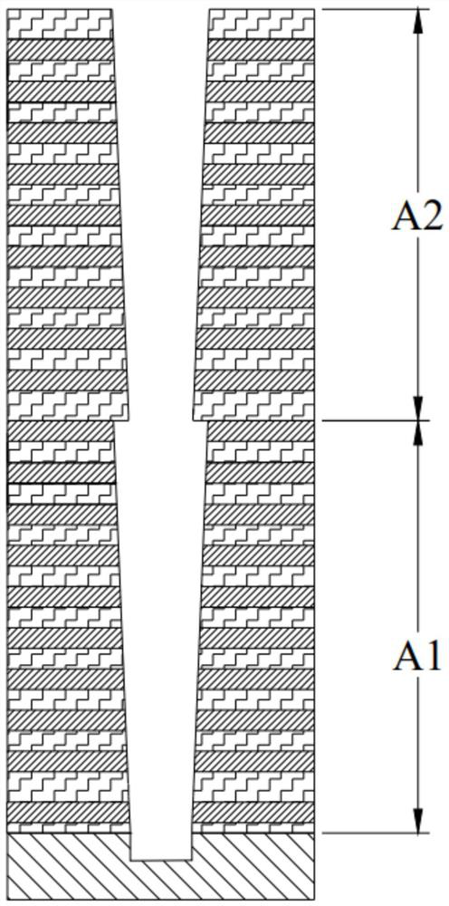
[0040] Three-dimensional (Three dimensional, 3D) stacking technology can form chips or structures with different functions through micromachining techniques such as stacking or hole interconnection to form a 3D three-dimensional memory chip with three-dimensional integration and signal communication in the vertical direction. Three-dimensional (3D) memory uses this technology to three-dimensionally arrange memory cells on a substrate to increase the storage density of the memory.

[0041] Three-dimensional (3D) memory includes 3D NOR (Nor Not) memory and 3D NAND (3D NAND) memory. Compared wit...


PUM


Abstract

The present application provides a three-dimensional memory and a preparation method thereof. The three-dimensional memory includes a substrate, a first stacking structure and a second stacking structure sequentially stacked on the substrate; the first stacking structure is arranged on the stacking surface of the substrate, and the first stacking structure has a For the bottom contact of the first sub-channel hole, the thickness of the first stack structure is the first thickness; the second stack structure is arranged on the surface of the first stack structure away from the substrate, and the second stack structure is provided with a For the second sub-channel hole connected to the first sub-channel hole, the thickness of the second stack structure is the second thickness, and the second thickness is smaller than the first thickness. The three-dimensional memory of the present application solves the problem that in the prior art, due to the increase in the number of stacked layers, the inclination of the channel hole in the upper layer becomes more and more serious, resulting in the inability to align with the channel hole in the lower layer, and then engraving the bottom of the channel hole in the subsequent During corrosion, it will cause sidewall damage and affect the electrical performance of the three-dimensional memory.

Description

technical field [0001] The invention relates to the technical field of semiconductors, in particular to a three-dimensional memory and a preparation method thereof. Background technique [0002] At present, in the preparation process of three-dimensional memory, the etching process of channel hole (CH) is one of the key processes in the various processes involved in three-dimensional memory. With the increase of the number of stacked layers, the channel hole The aspect ratio of etching is further increased. In order to etch the channel hole, the channel hole is etched through two stacking processes. In the existing two-stage molding process, the inclination of the channel holes in the upper layer will affect the alignment with the channel holes in the lower layer. Alignment of the channel holes, and subsequent etching of the bottom of the channel holes will cause sidewall damage and affect the electrical performance of the three-dimensional memory. Contents of the inventi...

Claims


Application Information

Patent Timeline
Patent Type & Authority Patents(China)
IPC IPC(8): H01L27/11517H01L27/11551H01L27/11563H01L27/11578
CPCH10B41/30H10B41/27H10B43/30H10B43/27
Inventor 刘隆冬王猛王孝进
Owner YANGTZE MEMORY TECH CO LTD
Why Eureka
Try Eureka