
Preparation method of laminated absorption layer of double-gradient band gap CIGS solar cell

A technology for solar cells and absorbing layers, applied in circuits, photovoltaic power generation, electrical components, etc., can solve the problems of reduced surface bandgap width, difficulty in controlling quaternary components, and affecting battery efficiency, etc., to achieve improved surface bandgap width, four-dimensional Easy element composition control and good battery uniformity

Pending Publication Date: 2020-05-08
PHOTON TECH KUNSHAN CO LTD
View PDF3 Cites 3 Cited by
  • Summary
  • Abstract
  • Description
  • Claims
  • Application Information

AI Technical Summary

Problems solved by technology

[0003] The first is a three-step co-evaporation process, that is, while maintaining a relatively high substrate temperature, four elements of copper, indium, gallium, and selenium are evaporated on the molybdenum film at the same time. The advantage of this method is that the Ga element can be controlled by the three-step process. The bandgap distribution in the absorbing layer ensures the IV performance of CIGS thin film solar cells, but the process is extremely complicated, and the components are extremely volatile during the preparation process, especially In and Se volatilize seriously, resulting in difficulty in controlling the quaternary components, which is very difficult. It is easy to cause the composition of the absorbing layer to be inconsistent with the ideal design composition, so its process uniformity and stability are very poor, especially for large-area components (area greater than 0.5m 2 ) when the yield drops sharply
[0004] The second is the prefabricated film selenization annealing process. First, the copper indium gallium selenium quaternary alloy target is used to sputter to form a film, and then the Se element is heated and volatilized into gas or H 2 Se gas is used to anneal the film. The advantages of this method are that the process is relatively simple, the quaternary composition is easy to control, and the composition uniformity and process stability are good. However, due to the low binding energy of In and Se during high temperature annealing, the binding energy of Ga and Se Higher, when the Se chemical reaction occurs, it gradually moves from the surface of the absorber layer to the inside of the absorber layer, so CuInSe is easily generated on the surface 2 , causing the surface layer Ga to easily diffuse to the back electrode, so the sharp drop in the surface Ga content will lead to a decrease in the surface bandgap width, making it impossible to form a double gradient bandgap, affecting the surface recombination and causing a drop in the open circuit voltage, which will eventually affect the overall battery efficiency.
Although in the prior art, a low Ga molar ratio target is used for bottom layer sputtering and a high Ga molar ratio target is used for surface layer sputtering, and then the selenization process is carried out, there is still a problem that CuInSe is easily formed on the surface. 2 The problem is that the surface layer Ga is easy to diffuse to the back electrode, the surface layer Ga content drops sharply, and it is impossible to form a double gradient band gap, and it is impossible to form a high-efficiency battery.

Method used


Image

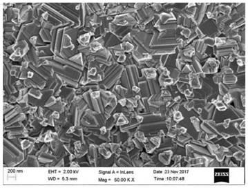
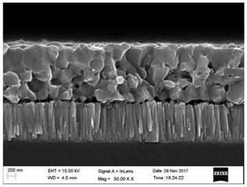
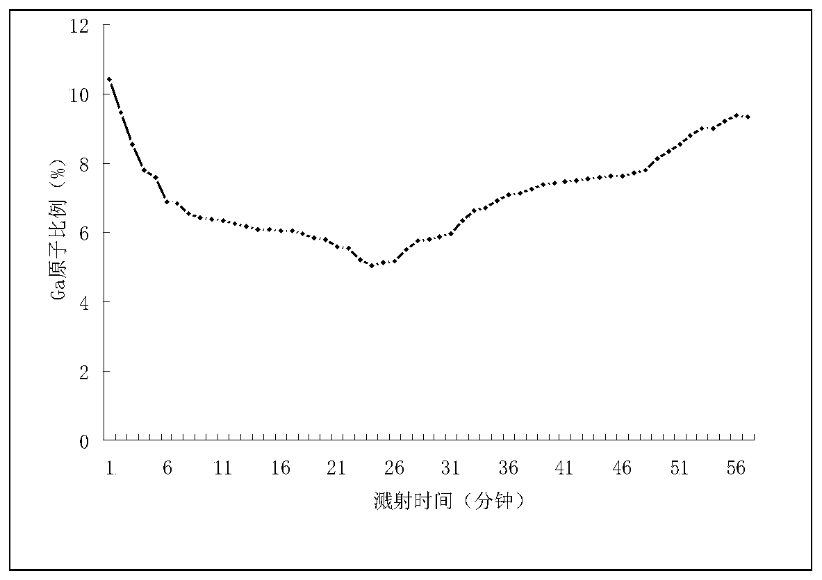
  • Preparation method of laminated absorption layer of double-gradient band gap CIGS solar cell
  • Preparation method of laminated absorption layer of double-gradient band gap CIGS solar cell
  • Preparation method of laminated absorption layer of double-gradient band gap CIGS solar cell

Examples


Embodiment 1

[0028] A method for preparing a laminated absorber layer of a dual gradient bandgap CIGS solar cell, the steps are as follows:

[0029] (1) First sputter 100nm thick SiO on the glass substrate 2 barrier layer.

[0030] (2) on SiO 2 Above the barrier layer, 800nm ​​thick metal Mo is sputtered, and Mo is the bottom electrode of the CIGS thin film battery.

[0031] (3) On the Mo electrode, use the quaternary Cu-In-Ga-Se alloy target to sputter to obtain the bottom layer of the thin film absorption layer, the molar ratio of the target is: Se / (Cu+In+Ga)=1.05; On the bottom layer of the absorbing layer, the surface layer of the thin film absorbing layer is obtained by sputtering with a quaternary Cu-In-Ga-Se alloy target, and the molar ratio of the target is: Se / (Cu+In+Ga)=0.95.

[0032] (4) The molar ratios of the bottom target materials are respectively: Cu / (In+Ga)=0.80, Ga / (In+Ga)=0.30, the chamber is evacuated, when the vacuum degree reaches the background vacuum 2*10 -3 Pa,...

Embodiment 2

[0042] A method for preparing a laminated absorber layer of a dual gradient bandgap CIGS solar cell, the steps are as follows:

[0043] (1) First sputter 100nm thick SiO on the glass substrate 2 barrier layer.

[0044] (2) on SiO 2 Above the barrier layer, 800nm ​​thick metal Mo is sputtered, and Mo is the bottom electrode of the CIGS thin film battery.

[0045] (3) On the Mo electrode, use the quaternary Cu-In-Ga-Se alloy target to sputter to obtain the bottom layer of the thin film absorption layer, the molar ratio of the target is: Se / (Cu+In+Ga)=1.00; On the bottom layer of the absorbing layer, the surface layer of the thin film absorbing layer is obtained by sputtering with a quaternary Cu-In-Ga-Se alloy target, and the molar ratio of the target is: Se / (Cu+In+Ga)=0.90.

[0046] (4) The molar ratios of the bottom target materials are respectively: Cu / (In+Ga)=0.80, Ga / (In+Ga)=0.30, the chamber is evacuated, when the vacuum degree reaches the background vacuum 2*10 -3 Pa,...

Embodiment 3

[0051] A method for preparing a laminated absorber layer of a dual gradient bandgap CIGS solar cell, the steps are as follows:

[0052] (1) First sputter 100nm thick SiO on the glass substrate 2 barrier layer.

[0053] (2) on SiO 2 Above the barrier layer, 800nm ​​thick metal Mo is sputtered, and Mo is the bottom electrode of the CIGS thin film battery.

[0054] (3) On the Mo electrode, first sputter the underlying film of the quaternary Cu-In-Ga-Se alloy target, and the molar ratios are: Se / (Cu+In+Ga)=1.09, Cu / (In+Ga )=0.80, Ga / (In+Ga)=0.30; followed by sputtering the quaternary Cu-In-Ga-Se alloy target surface film, the molar ratios are respectively: Se / (Cu+In+Ga)=0.99, Cu / (In+Ga)=0.80, Ga / (In+Ga)=0.30. Two layers of films form an absorbing layer stack, and the sputtering thicknesses of the corresponding bottom film and surface film are both 0.75 μm.

[0055] (4) Vacuum the vacuum annealing furnace before heating, when the vacuum degree reaches the background vacuum 5*1...


PUM

PropertyMeasurementUnit
thicknessaaaaaaaaaa
thicknessaaaaaaaaaa
thicknessaaaaaaaaaa

Abstract

The invention discloses a preparation method of a laminated absorption layer of a double-gradient band gap CIGS solar cell, and the method comprises the following steps: (1) preparing a thin film absorption layer bottom layer on an electrode through a quaternary Cu-In-Ga-Se target material, wherein the molar ratio of the target material is Se / (Cu + In + Ga) = 1.00-1.30; (2), preparing a thin filmabsorption layer surface layer on the absorption layer bottom layer through a quaternary Cu-In-Ga-Se target material, wherein the molar ratio of the target material is as follows: Se / (Cu + In + Ga) =0.75-0.99. According to the invention, a prefabricated film selenylation process is adopted, sputtering is carried out on two target materials with different selenium molar ratios, and then a high-temperature selenylation annealing process is carried out, so the bottom layer is rich in selenium to promote crystal growth and realize high short-flow density; the problem of low width of a surface band gap is solved due to surface selenium deficiency, and a double-gradient band gap, high open-circuit voltage, a high filling factor and a high-efficiency battery are realized.

Description

technical field [0001] The invention relates to a preparation technology of CIGS thin-film solar cell materials, in particular to a preparation method of a laminated absorbing layer of a CIGS solar cell with double gradient band gaps. Background technique [0002] At present, there are two mainstream methods for preparing the absorber layer of copper indium gallium selenium thin film solar cells for industrial application. They are three-step co-evaporation method and pre-film selenization annealing process. [0003] The first is a three-step co-evaporation process, that is, while maintaining a relatively high substrate temperature, four elements of copper, indium, gallium, and selenium are evaporated on the molybdenum film at the same time. The advantage of this method is that the Ga element can be controlled by the three-step process. The bandgap distribution in the absorbing layer ensures the IV performance of CIGS thin film solar cells, but the process is extremely comp...

Claims


Application Information

Patent Timeline
Patent Type & Authority Applications(China)
IPC IPC(8): H01L21/363H01L31/032H01L31/18
CPCH01L21/02568H01L21/02631H01L21/02664H01L31/18H01L31/0322Y02P70/50Y02E10/541
Inventor 王鹏张亚飞张伟
Owner PHOTON TECH KUNSHAN CO LTD
Learn More